POLY-Si THIN FILM TRANSISTOR AND ORGANIC LIGHT-EMITTING DISPLAY HAVING THE SAME

a thin film transistor and organic technology, applied in the direction of basic electric elements, electrical equipment, semiconductor devices, etc., can solve the problems of reduced yield, high current leakage rate through the tft, complicated doping process, etc., and achieve the effect of effectively reducing the leakage curren

Active Publication Date: 2007-06-07
SAMSUNG ELECTRONICS CO LTD
View PDF5 Cites 169 Cited by
  • Summary
  • Abstract
  • Description
  • Claims
  • Application Information

AI Technical Summary

Benefits of technology

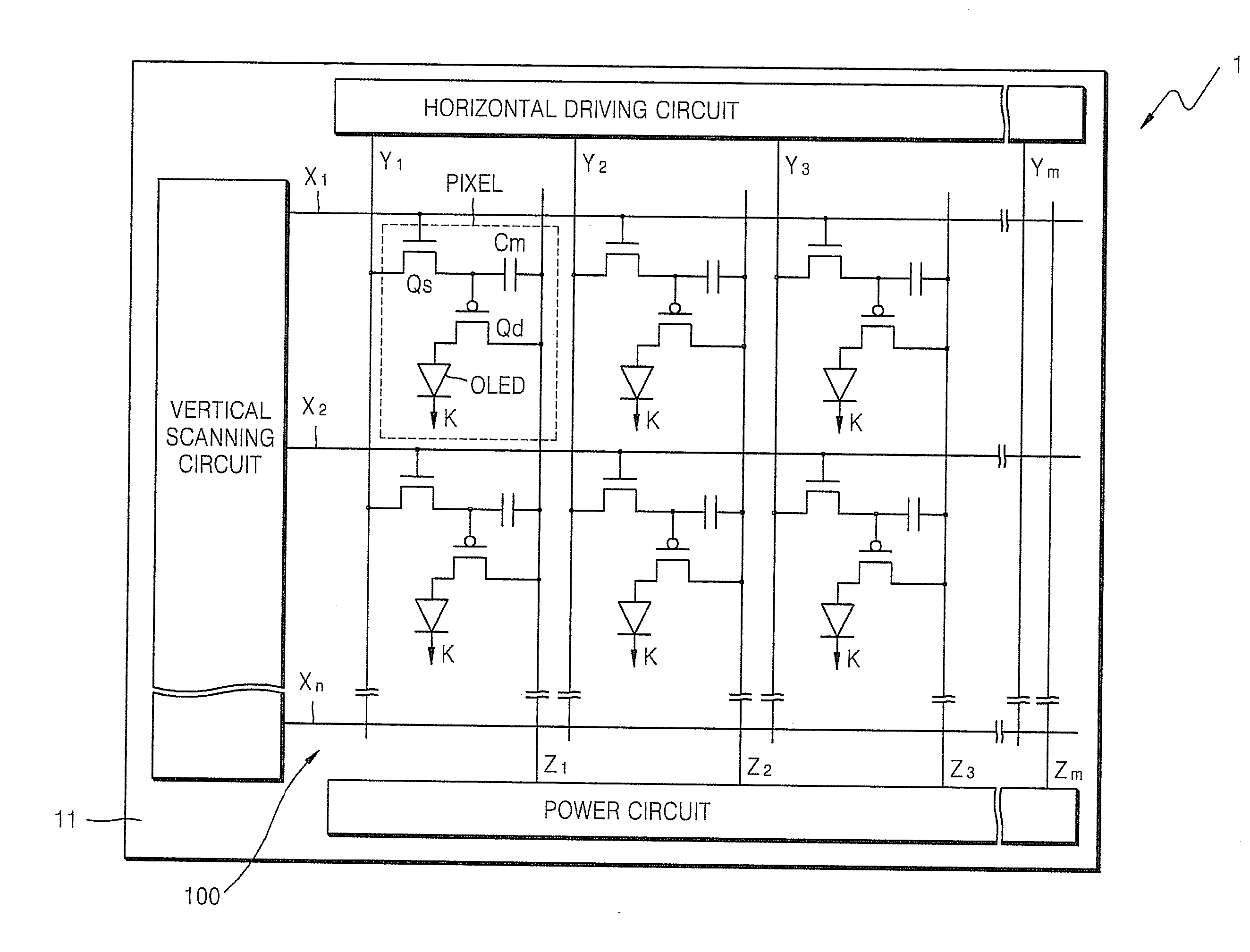
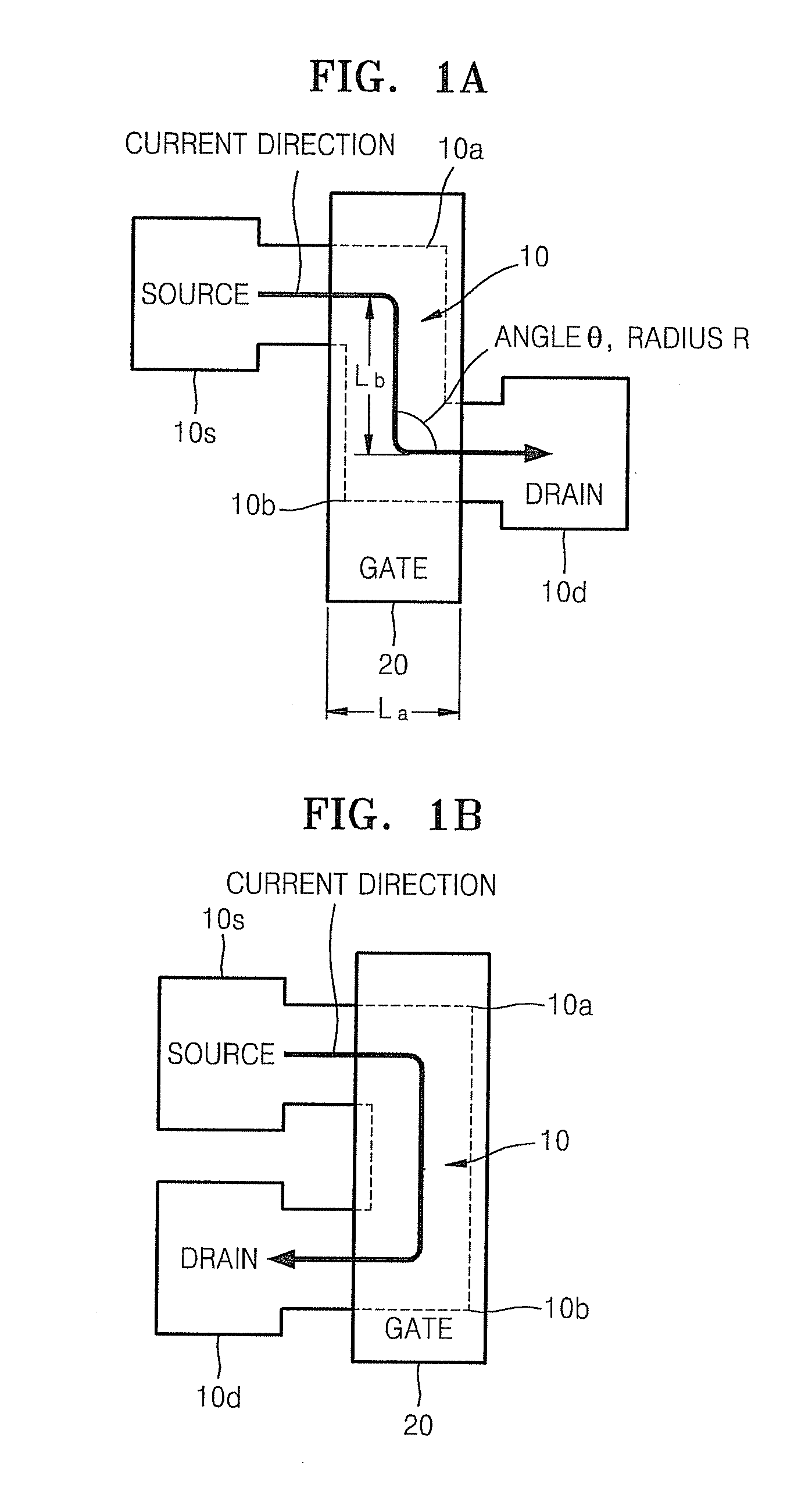
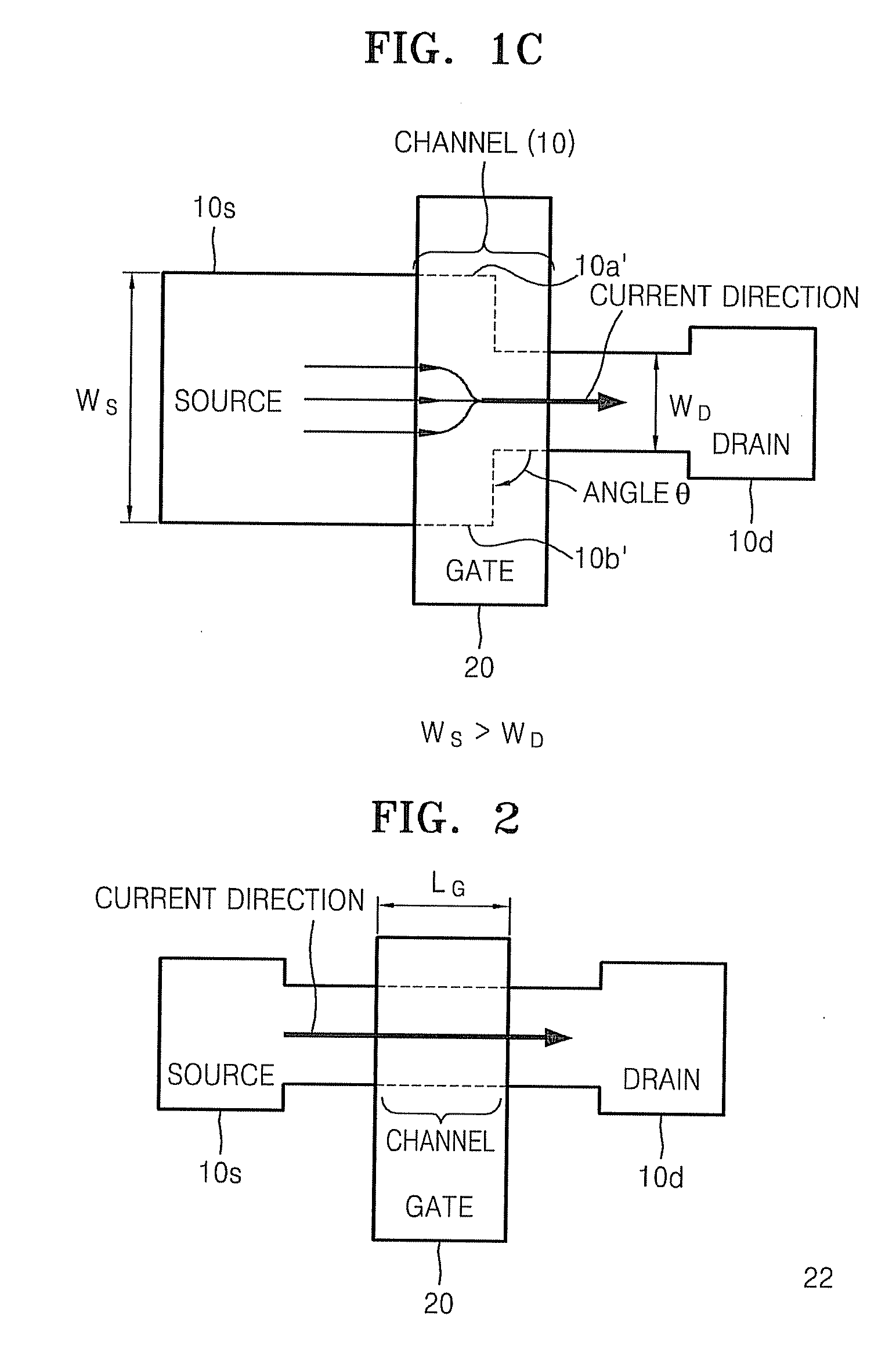
[0010] The present invention provides a polycrystalline silicon (“p-Si”) thin film transistor (“TFT”) which has properly-adjusted electron mobility so that a leakage current can be effectively reduced, and an organic light-emitting display having the same.

Problems solved by technology

One of the disadvantages of a p-Si TFT includes a high rate of current leakage through the TFT when an off signal is sent to the gate terminal thereof.
However, since an additional mask is used in the above method, the doping process becomes more complicated, yield is reduced and productivity is lowered.
However, the size of a light-emitting region within a pixel is of a limited area and a larger gate inevitably reduces that area and therefore the luminous efficiency of a device using large gates is lowered.
Alternative methods of reducing the leakage current such as fabricating a dual gate TFT are complicated and manufacturing costs thereof are high.
In an OLED, although reduction in a leakage current using an additional circuit in each switching TFT of a pixel is possible, the additional circuit includes an additional device such as a TFT, thus increasing manufacturing costs greatly.

Method used


Image

  • POLY-Si THIN FILM TRANSISTOR AND ORGANIC LIGHT-EMITTING DISPLAY HAVING THE SAME
  • POLY-Si THIN FILM TRANSISTOR AND ORGANIC LIGHT-EMITTING DISPLAY HAVING THE SAME
  • POLY-Si THIN FILM TRANSISTOR AND ORGANIC LIGHT-EMITTING DISPLAY HAVING THE SAME

Examples


Embodiment Construction

[0024] Hereinafter, the present invention will be described more fully with reference to the accompanying drawings, in which exemplary embodiments of the invention are shown. This invention may, however, be embodied in many different forms and should not be construed as limited to the exemplary embodiments set forth herein. Rather, these embodiments are provided so that this disclosure will be thorough and complete, and will fully convey the scope of the invention to those skilled in the art. In the drawings, lengths and sizes of layers and regions may be exaggerated for clarity.

[0025] It will be understood that when an element or layer is referred to as being “on” another element or layer, the element or layer can be directly on another element or layer or intervening elements or layers. In contrast, when an element is referred to as being “directly on” another element or layer, there are no intervening elements or layers present. Like numbers refer to like elements throughout. As...


PUM


Abstract

A thin film transistor comprises an Si-based channel having a nonlinear electron-moving path, a source and a drain disposed at both sides of the channel, a gate disposed above the channel, an insulator interposed between the channel and the gate, and a substrate supporting the channel and the source and the drain disposed at either side of the channel respectively.

Description

[0001] This application claims priority to Korean Patent Application No. 10-2005-0116887, filed on Dec. 2, 2005, and all the benefits accruing therefrom under 35 U.S.C. § 119, the contents of which in its entirety are herein incorporated by reference. BACKGROUND OF THE INVENTION [0002] 1. Field of the Invention [0003] The present invention relates to a poly-Si thin film transistor (“TFT”) and an organic light-emitting display having the same. [0004] 2. Description of the Related Art [0005] Polycrystalline silicon (“p-Si”) has higher electron mobility than that of amorphous silicon (“a-Si”) and has good optical stability. P-Si has been widely used in a variety of fields, and in particular, in thin film transistors (“TFTs”) or memory devices. P-Si TFTs have been used as switching devices in display devices, for example. Display devices using an active device such as a TFT include TFT liquid crystal displays (“LCDs”) and TFT organic light-emitting displays (“OLEDs”). [0006] TFT LCDs or...

Claims


Application Information

Patent Timeline
Patent Type & Authority Applications(United States)
IPC IPC(8): H01L21/84H01L27/12
CPCH01L27/12H01L29/78609H01L29/78696H10K59/12
Inventor YIN, HUAXIANGNOGUCHI, TAKASHILIM, HYUKXIANYU, WENXUCHO, HANS S.
Owner SAMSUNG ELECTRONICS CO LTD
Why Eureka
Try Eureka