Three dimensional non-volatile storage with dual gate selection of vertical bit lines

a non-volatile storage and vertical bit line technology, applied in the field of non-volatile storage, can solve the problems of reading or programming voltages being applied to a very large number of other memory elements

Active Publication Date: 2012-06-14
SANDISK TECH LLC
View PDF4 Cites 157 Cited by
  • Summary
  • Abstract
  • Description
  • Claims
  • Application Information

AI Technical Summary

Problems solved by technology

The desire to perform data reading and programming operations with a large number of memory elements in parallel results in reading or programming voltages being applied to a very large number of other memory elements.

Method used


Image

  • Three dimensional non-volatile storage with dual gate selection of vertical bit lines
  • Three dimensional non-volatile storage with dual gate selection of vertical bit lines
  • Three dimensional non-volatile storage with dual gate selection of vertical bit lines

Examples


Embodiment Construction

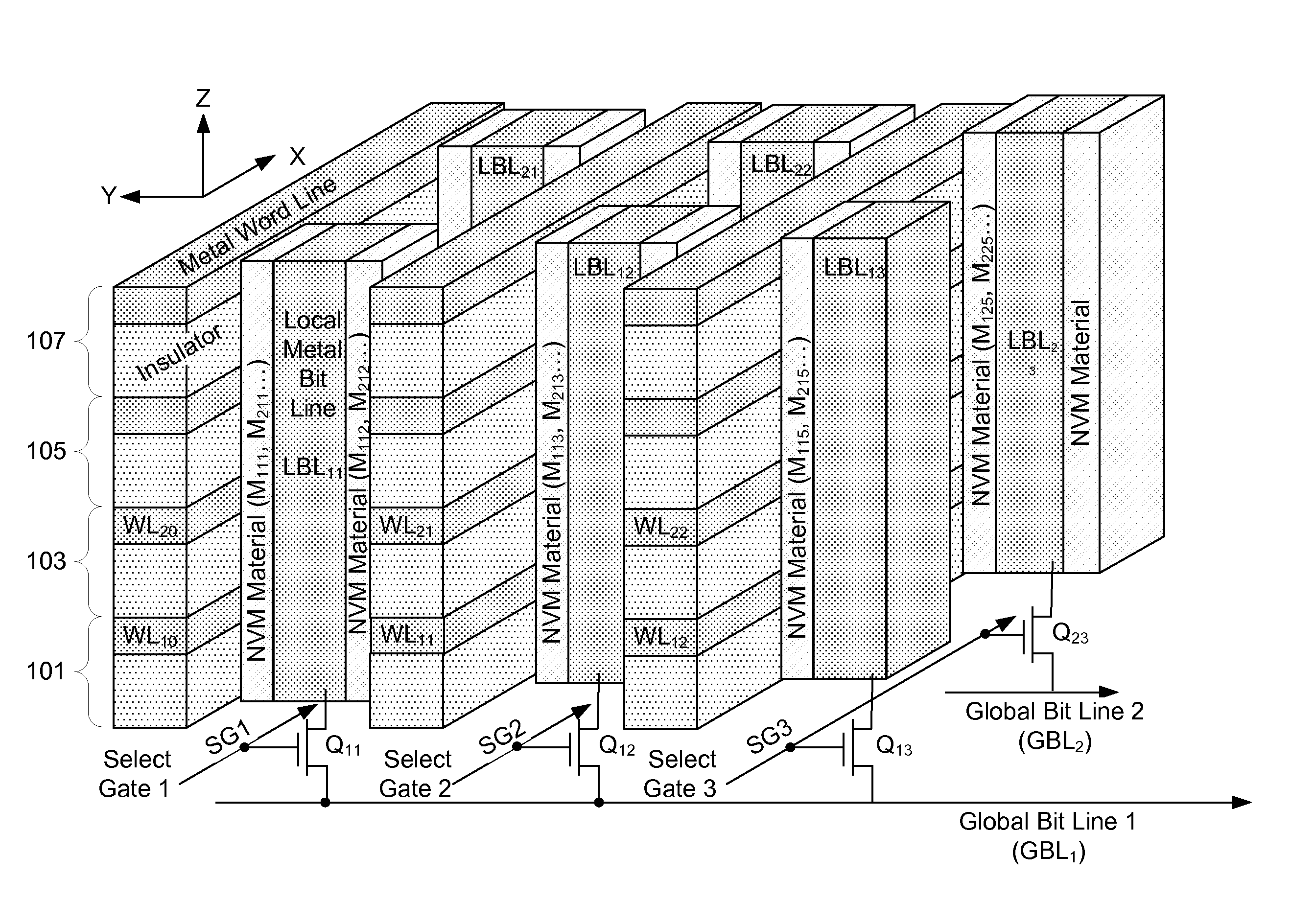
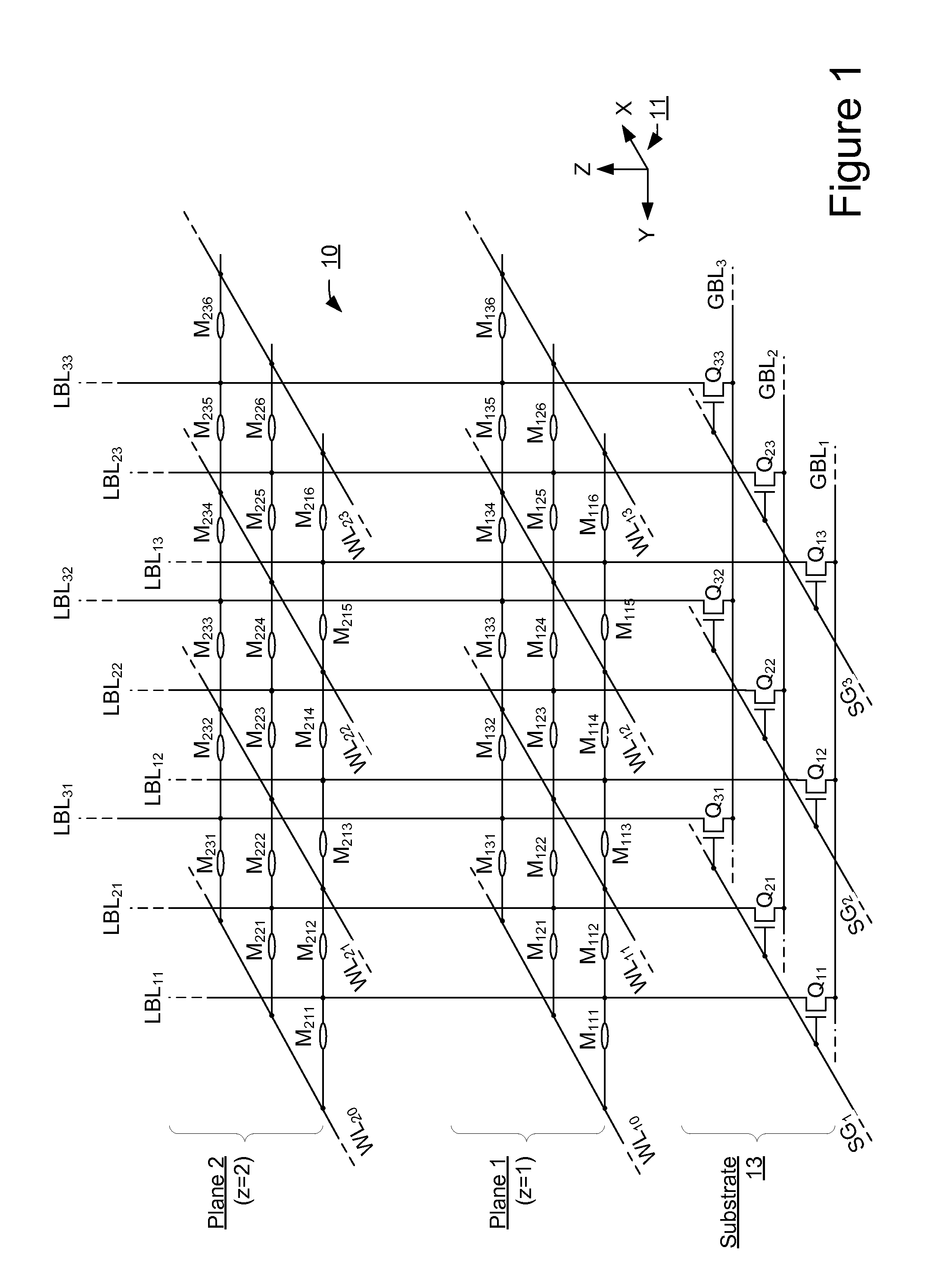
[0049]The technology described herein is directed to an architecture for a three-dimensional array of memory elements wherein bit lines of the array are oriented vertically. That is, instead of merely stacking a plurality of existing two-dimensional arrays on a common semiconductor substrate, where each two-dimensional array has its own bit lines, multiple two-dimensional arrays are stacked on top of each other in separate planes but then share common bit lines that extend up through the planes.

[0050]The memory elements used in the three-dimensional array are preferably variable resistive memory elements. That is, the resistance (and thus inversely the conductance) of the individual memory elements is typically changed as a result of a voltage placed across the orthogonally intersecting conductors to which the memory element is connected. Depending on the type of variable resistive element, the state may change in response to a voltage across it, a level of current though it, an amo...


PUM


Abstract

A three-dimensional array adapted for memory elements that reversibly change a level of electrical conductance in response to a voltage difference being applied across them. Memory elements are formed across a plurality of planes positioned different distances above a semiconductor substrate. Bit lines to which the memory elements of all planes are connected are oriented vertically from the substrate and through the plurality of planes.

Description

[0001]This application claims the benefit of U.S. Provisional Application 61 / 526,764, “Optimizing Architecture for Three Dimensional Non-Volatile Storage Device With Vertical Bit Lines,” filed on Aug. 24, 2011 and U.S. Provisional Application 61 / 423,007, “Non-Volatile Memory Having 3D Array of Read / Write Elements With Vertical Bit Lines and Laterally Aligned Active Elements and Methods Thereof,” filed on Dec. 14, 2010, both application are incorporated herein by reference in their entirety.BACKGROUND OF THE INVENTION[0002]1. Field of the Invention[0003]The present invention relates to technology for non-volatile storage.[0004]2. Description of the Related Art[0005]One example of non-volatile memory uses variable resistance memory elements that may be set to either low or high resistance states, and can remain in that state until subsequently re-set to the initial condition. The variable resistance memory elements are individually connected between two orthogonally extending conducto...

Claims


Application Information

Patent Timeline
Patent Type & Authority Applications(United States)
IPC IPC(8): G11C5/02G11C7/00
CPCG11C13/0002G11C8/08H01L45/1226H01L45/146H01L27/2454H01L27/249H01L27/115H01L27/0688H01L27/2481H01L27/2463H01L45/1233G11C13/0026G11C5/025G11C13/0028H01L45/165H01L45/1683H01L45/08H10B63/34H10B63/845H10N70/20H10N70/823H10N70/8833G11C16/24G11C16/06G11C16/08G11C13/0033G11C13/0069H10B69/00H10B63/80H10B63/84H10N70/043H10N70/066H10N70/826H10N70/24
Inventor SCHEUERLEIN, ROY E.
Owner SANDISK TECH LLC
Why Eureka
Try Eureka