Logic circuit and semiconductor device

a logic circuit and semiconductor technology, applied in the field of logic circuits, can solve the problems of static power consumption due to leakage current cannot be reduced, power consumption cannot be reduced, power consumption, etc., and achieve the effects of reducing the standby power of logic circuits, reducing the concentration of hydrogen, and reducing the leakage current of transistors

Active Publication Date: 2012-06-26
SEMICON ENERGY LAB CO LTD
View PDF199 Cites 175 Cited by
  • Summary
  • Abstract
  • Description
  • Claims
  • Application Information

AI Technical Summary

Benefits of technology

[0008]By the above-described clock gating, dynamic power consumed can be reduced, but the static power consumed due to leakage current cannot be reduced. Note that the dynamic power consumed in the non-operating circuit includes power consumed due to charge and discharge of parasitic capacitor formed by wirings to which a clock signal is supplied. Further, in the circuit where clock gating is performed, the state of an element included in the non-operating circuit is held. Thus, power consumed due to the leakage current of the transistor accounts for a large percent of the standby power. In addition, the probability of malfunction of the logic circuit, caused by leakage current of the transistor, becomes high.
[0009]In view of the above problem, one of objects of one embodiment of the present invention is to reduce standby power due to leakage current or suppress malfunction in a logic circuit performing clock gating.
[0013]By using a highly-purified oxide semiconductor as described for a channel formation region, a transistor whose channel width is even 10 mm has a drain current of 1×10⁻¹³ [A] or lower in the case where the drain voltage is 1 V and 10 V and the gate voltage is in the range of −5 V to −20 V. In other words, a highly-purified oxide semiconductor is used for a channel formation region of a transistor, whereby leakage current can be drastically reduced.
[0015]The logic circuit of one embodiment of the present invention includes a transistor which is in an off state where a potential difference exists between a source terminal and a drain terminal over a period during which a clock signal is not supplied. A channel formation region of the transistor is formed using an oxide semiconductor in which the hydrogen concentration is reduced. Specifically, the hydrogen concentration of the oxide semiconductor is 5×10¹⁹ (atoms / cm3) or lower. Therefore, leakage current of the transistor can be reduced. As a result, the standby power of the logic circuit can be reduced and malfunction of the logic circuit can be suppressed.
[0016]In particular, in the logic circuit where clock gating is performed, a state in the logic circuit is held for a long time. That is, a specific transistor keeps an off state for a long time, where a potential difference exists between a source terminal and a drain terminal. Applying such a transistor to the above transistor brings great effect.
[0017]Further, reduction in power consumed in the whole circuit allows reduction in loads of an external circuit which makes a logic circuit of one embodiment of the present invention operate. Thus, the functionality of a semiconductor device including the logic circuit and the external circuit can be expanded.

Problems solved by technology

By the above-described clock gating, dynamic power consumed can be reduced, but the static power consumed due to leakage current cannot be reduced.
Thus, power consumed due to the leakage current of the transistor accounts for a large percent of the standby power.
In addition, the probability of malfunction of the logic circuit, caused by leakage current of the transistor, becomes high.

Method used


Image

  • Logic circuit and semiconductor device
  • Logic circuit and semiconductor device
  • Logic circuit and semiconductor device

Examples


embodiment 1

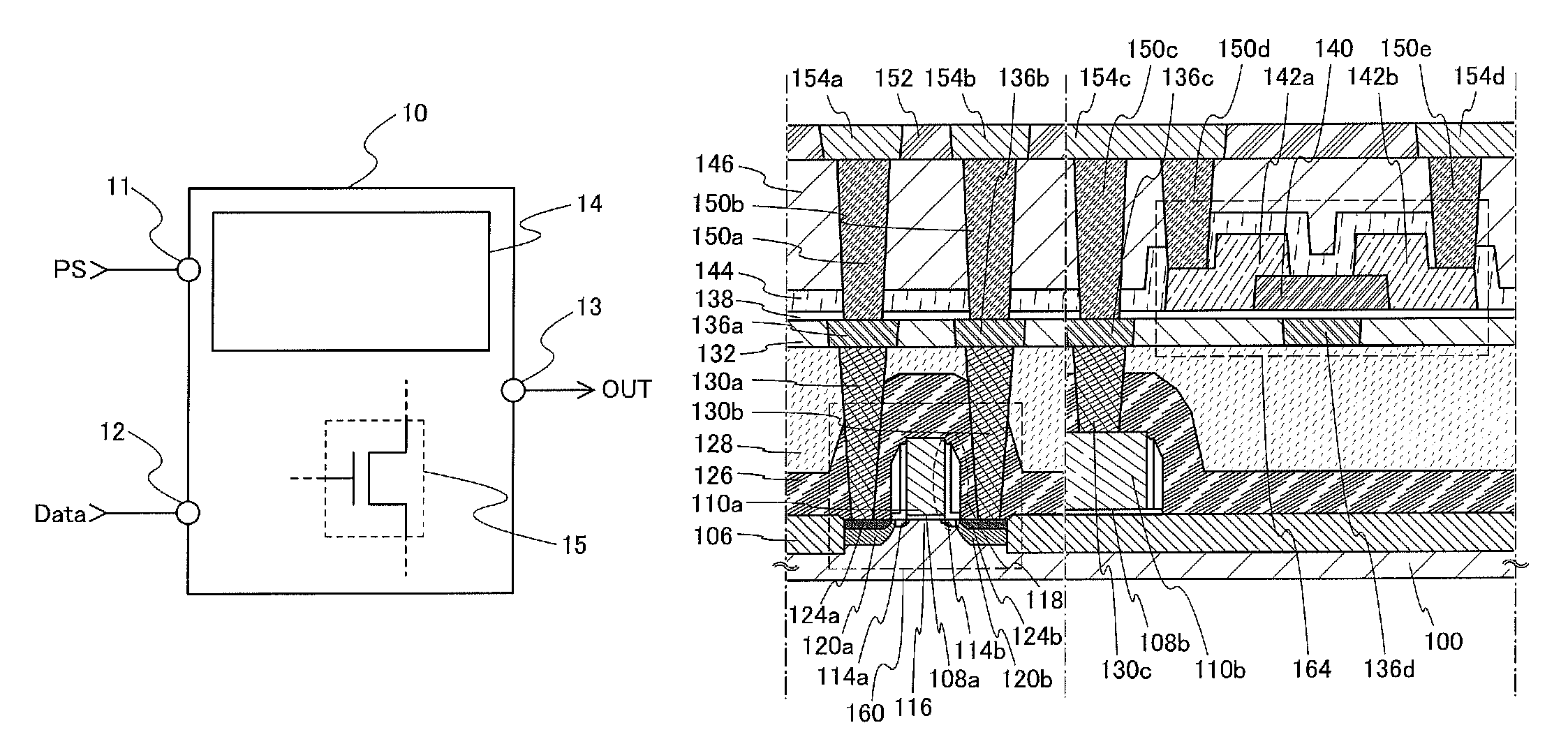
[0047]In this embodiment, an example of a logic circuit where clock gating is performed will be described. Specifically, an example of a logic circuit having a period during which a clock signal is input and a period during which a clock signal is not input and performing arithmetic processing with use of the clock signal will be described with reference to FIG. 1.

[0048]A logic circuit 10 shown in FIG. 1 includes a first input terminal 11 electrically connected to a wiring through which a pulse signal (PS) is supplied (hereinafter, also referred to as a pulse signal line), a second input terminal 12 electrically connected to a wiring through which a data signal (Data) is supplied (hereinafter, also referred to as a data signal line), and an output terminal 13. The logic circuit 10 has a period during which a clock signal (CK) is supplied through the pulse signal line and a period during which a clock signal is not supplied. That is, the logic circuit shown in FIG. 1 is a logic circu...

embodiment 2

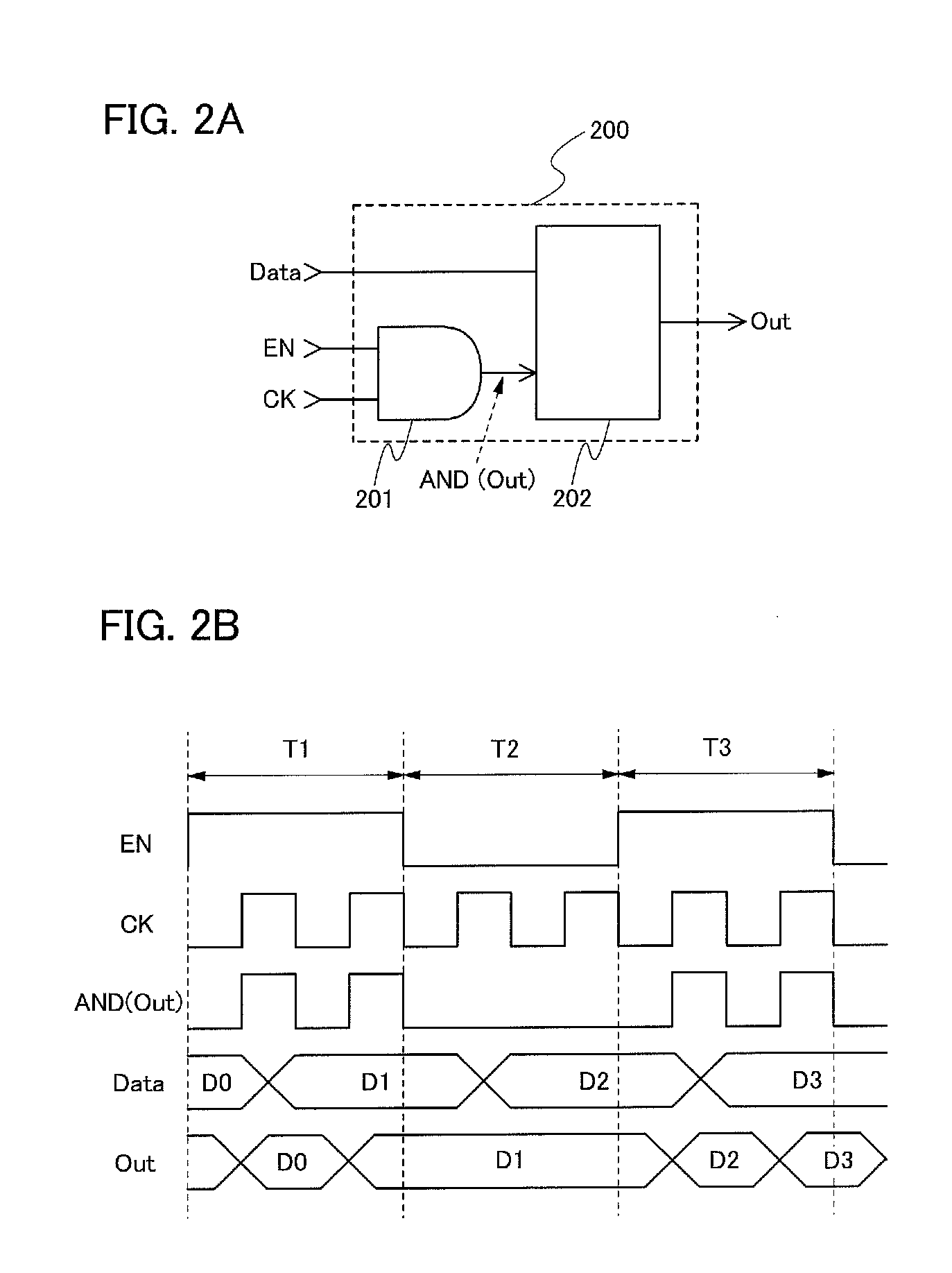
[0055]In this embodiment, an example of the logic circuit described in Embodiment I will be described. Specifically, a logic circuit including an AND gate and a flip-flop will be described with reference to FIGS. 2A and 2B, FIGS. 3A and 3B, and FIGS. 4A to 4C.

[0056]A logic circuit 200 of this embodiment shown in FIG. 2A includes an AND gate 201 and a flip-flop 202. The AND gate 201 has a first input terminal which is electrically connected to a wiring through which an enable signal (EN) is supplied (hereinafter, also referred to as an enable signal line) and a second input terminal which is electrically connected to a wiring through which a clock signal (CK) is supplied (hereinafter, also referred to as a clock signal line). The flip-flop 202 has a first input terminal which is electrically connected to a data signal line and a second input terminal which is electrically connected to an output terminal of the AND gate 201.

[0057]Note that the flip-flop 202 included in the logic circu...

embodiment 3

[0107]In this embodiment, an example of the logic circuit described in Embodiment I will be described. Specifically, a logic circuit including a NOR gate and a flip-flop will be described with reference to FIGS. 5A and 5B and FIGS. 6A and 6B.

[0108]A logic circuit 500 of this embodiment shown in FIG. 5A includes a NOR gate 501 and a flip-flop 502. In the NOR gate 501, a first input terminal is electrically connected to an enable signal line and a second input terminal is electrically connected to a wiring through which an inverted circuit signal (CKB) is supplied (hereinafter, also referred to as an inverted clock signal line). In the flip-flop 502, a first input terminal is electrically connected to a data signal line and a second input terminal is electrically connected to an output terminal of the NOR gate 501.

[0109]Note that the flip-flop 502 included in the logic circuit of this embodiment is a circuit which can retain data for one bit utilizing feedback operation. An output sig...


PUM


Abstract

In a logic circuit where clock gating is performed, the standby power is reduced or malfunction is suppressed. The logic circuit includes a transistor which is in an off state where a potential difference exists between a source terminal and a drain terminal over a period during which a clock signal is not supplied. A channel formation region of the transistor is formed using an oxide semiconductor in which the hydrogen concentration is reduced. Specifically, the hydrogen concentration of the oxide semiconductor is 5×10¹⁹ (atoms / cm3) or lower. Thus, leakage current of the transistor can be reduced. As a result, in the logic circuit, reduction in standby power and suppression of malfunction can be achieved.

Description

TECHNICAL FIELD[0001]The present invention relates to a logic circuit, particularly, a logic circuit including a transistor in which a channel formation region is formed using an oxide semiconductor. The present invention also relates to a semiconductor device including the logic circuit.[0002]Note that a semiconductor device in this specification refers to all devices which can function by utilizing semiconductor characteristics, and electro-optical devices, semiconductor circuits, and electronic appliances are all semiconductor devices.BACKGROUND ART[0003]In a general circuit including transistors manufactured by using a Si wafer or SOI (silicon on insulator), as the operation voltage is reduced by progress of microfabrication, consumed power is reduced.[0004]Consumed power is a sum of dynamic power and static power (hereinafter, also referred to as standby power): the dynamic power is power consumed mainly by charge and discharge of the gate capacitor of transistors and the paras...

Claims


Application Information

Patent Timeline
Patent Type & Authority Patents(United States)
IPC IPC(8): H03K19/096
CPCH01L27/1225H03K3/0375H03K19/096H01L27/088H01L29/7869H03K19/0016Y02D10/00
Inventor SHIONOIRI, YUTAKAKOBAYASHI, HIDETOMO
Owner SEMICON ENERGY LAB CO LTD
Why Eureka
Try Eureka