Method and apparatus for on-the-fly minimum power state transition

Inactive Publication Date: 2008-10-02
GLOBALFOUNDRIES INC
View PDF9 Cites 20 Cited by
  • Summary
  • Abstract
  • Description
  • Claims
  • Application Information

AI Technical Summary

Benefits of technology

[0011]To that end, the present invention provides a novel improved input vector control (IVC) approach that may be referred to as “on-the-fly minimum power transition.” The novel “on-the-fly minimal power transition” method takes advantage of the fact that large portions of microprocessor logic is comprised of pipelines and quiescent functional units that need not be restored to their pre-sleep mode state when exiting from low power or sleep mode states. In many cases, it is sufficient to reset latches with the same logical values that the flip-flops are set to at initialization. Hence, the inventive structure and method takes advantage of existing logic circuits for initialization. This invention inserts an IVC circuit in IC scan path to apply the input vector to be set for IVC in just one cycle. The IVC circuit also allows to exit sleep mode and reinitialize the latch in one additional cycle. This reduces the power consumption required to enter and exit the sleep mode. The area

Problems solved by technology

Leakage power consumption is becoming an increasing problem for semiconductor designers as they pack larger amounts of transistors onto a single semiconductor integrated circuit (IC) or chip comprising a very large scale integrated (VLSI) circuit design.
VLSI designs, e.g., a microprocessor, display significant static power consumption through internal current leakage with three main sources.
One example where the toll in power consumption by this static leakage is readily apparent is in microprocessors where more than 30% of the total power consumed during normal operation is due to leakage.
Power leakage reduction in VLSI processors is not just an issue for operation and performance, but in manufacturing as well.
For that matter, leakage power consumption for normal operation causes a secondary power consumption in energy to cool the IC as a consequence.
If not cooled, increased temperature conditions can degrade IC performance and reliability.
The cited references appear to agree that leakage power consumption within an IC device depends strongly on the state of the IC device input and of the internal memory elements (e.g. latches), which affects switching and leakage significantly.
The Abdollahi approach, however, has its drawbacks.
For example, the suggested approach in

Method used


Image

  • Method and apparatus for on-the-fly minimum power state transition
  • Method and apparatus for on-the-fly minimum power state transition
  • Method and apparatus for on-the-fly minimum power state transition

Examples


Example

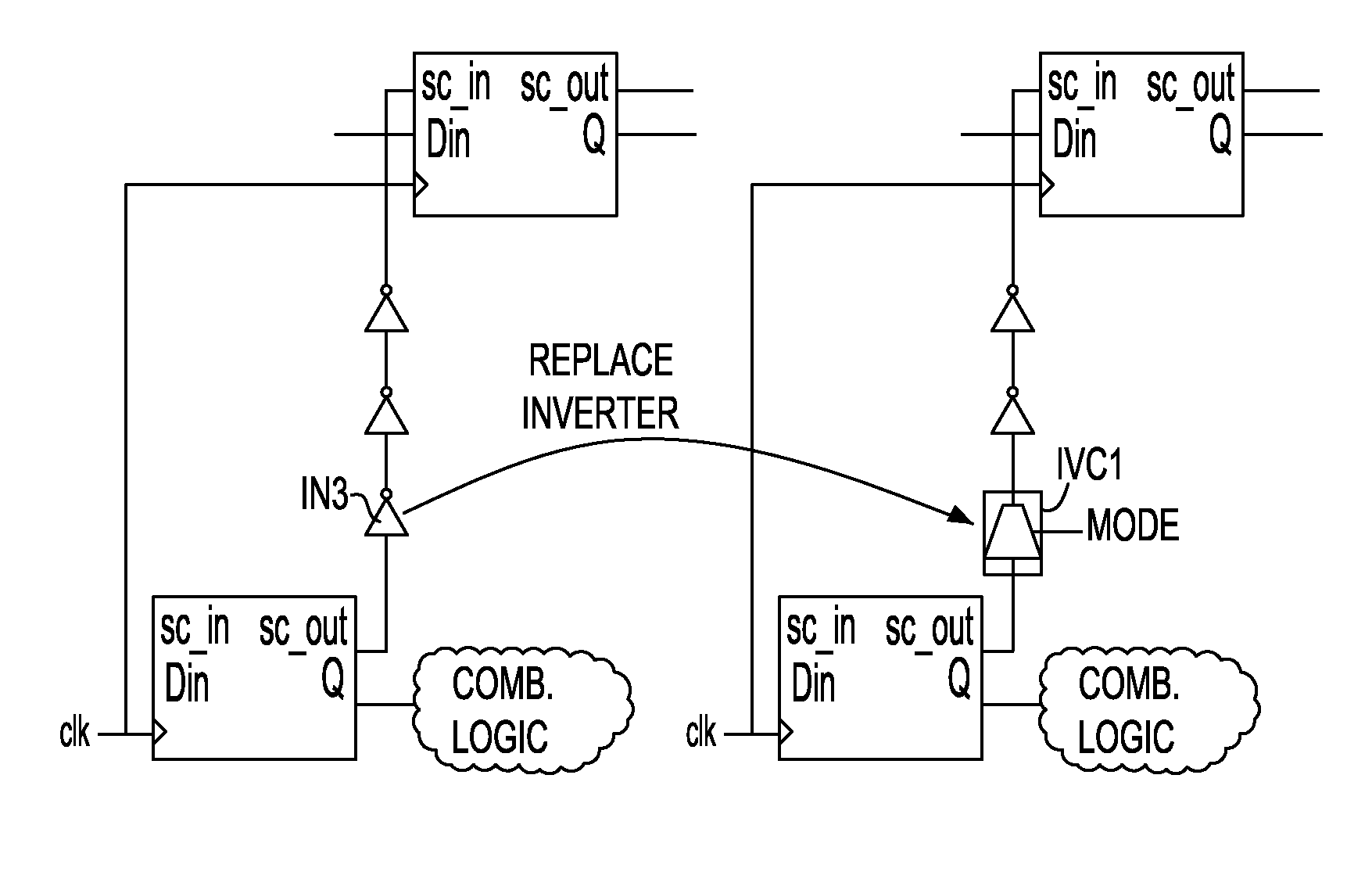
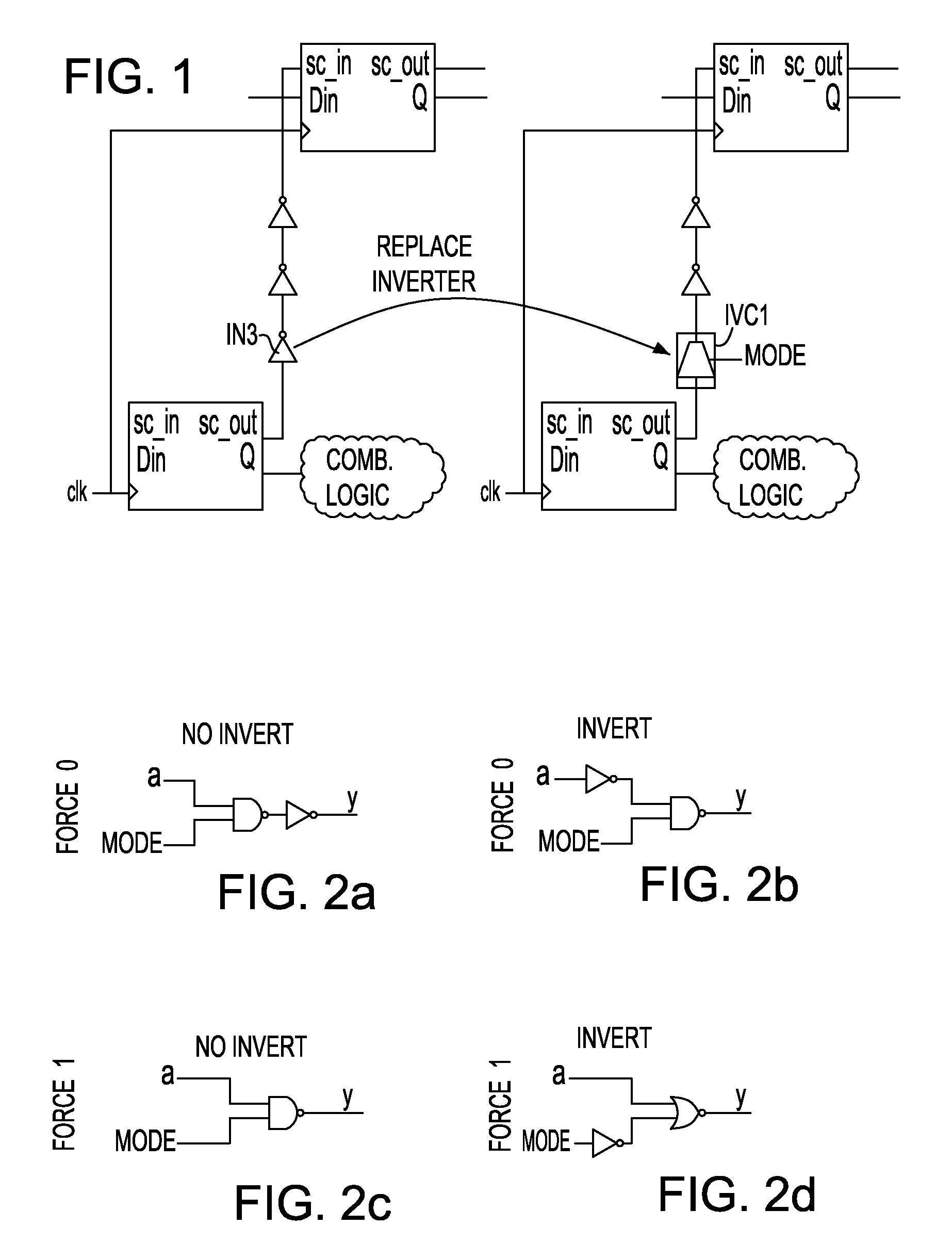
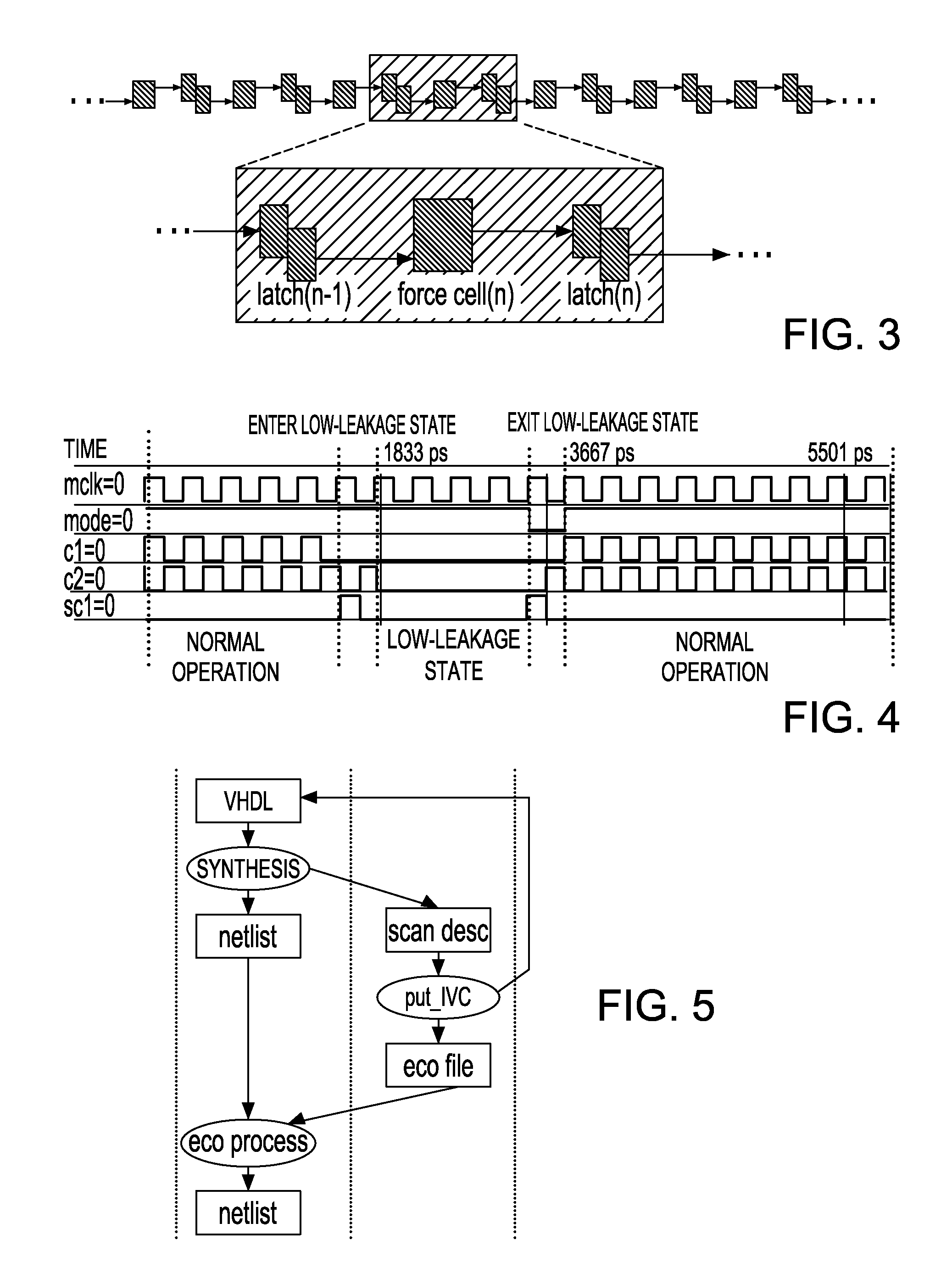
[0018]At initialization, many conventional VLSI designs, i.e., microprocessors, do not initialize their flip-flops with a global reset, which would require routing a global signal and consequential degrading of the flip-flop timing. Such conventional designs instead use the scan-path to force an initial value at flip-flops, such as that design disclosed in commonly owned U.S. Pat. No. 7,100,144. Hence, in order to reset N latches, the conventional scan-path approaches require circa N clock cycles. The drawback is that where N is very large (which it is in many typical VLSI microprocessor designs), initialization time becomes critical, particularly in certain applications (e.g., Telco market, real time applications, etc).

[0019]The inventive method and VLSI scan chain structure disclosed herein provide for an improved level sensitive scan design (LSSD) or scan-path approach. The novel approach may be described broadly as “on-the-fly minimum power transition”. The “on-the-fly minimum p...


PUM


Abstract

The invention includes a novel scan chain structure for LSSD or GSD IC operation. The scan chain structure includes a first flip-flop (L1) and a second flip-flop (L2) configured to operate the first flip-flop (L1) in normal mode operation, in scan mode operation, in initialization mode and in low leakage power mode operation, wherein each flip-flop within a long scan chain of latches includes a data input, data output, a clock input, a scan-in input and a scan-out output, arranged for normal mode operation. A buffer circuit is electrically connected between the scan-out output of the second flip-flop (L2) and the scan-in input of the first flip-flop (L1) for the next latch in the scan chain, the buffer circuit including a control element that controls the operation the first flip-flop (L1) to scan mode or low power leakage mode. The first flip-flop (L1) is set to a data output value upon exit from low power leakage mode that is the same value that it is set to at initialization during normal mode operation. The switching occurs in only one clock cycle.

Description

BACKGROUND OF THE INVENTION[0001]The present invention relates to improved power leakage control in very large scale integrated (VLSI) circuits, and more particularly relates to an improved input vector control (IVC) approach in a scan-based VLSI design that utilizes scan-chain logic to set sleep mode and reset the flip flops from a low-power state with the same logical values that the flip-flops were set to at initialization.[0002]Leakage power consumption is becoming an increasing problem for semiconductor designers as they pack larger amounts of transistors onto a single semiconductor integrated circuit (IC) or chip comprising a very large scale integrated (VLSI) circuit design. VLSI designs, e.g., a microprocessor, display significant static power consumption through internal current leakage with three main sources. The two main sources include: gate direct tunneling leakage and sub-threshold leakage through the channel of an “off” transistor. One example where the toll in power...

Claims


Application Information

Patent Timeline
IPC IPC(8): H03B21/00
CPCG01R31/318541G01R31/318575
Inventor ORTIZ, ALBERTO GARCIALICHTENAU, CEDRICROHRER, NORMAN J.
Owner GLOBALFOUNDRIES INC
Why Eureka
Try Eureka