Slew rate controlled output buffer

a buffer circuit and output buffer technology, applied in logic circuits, voltage/current interference elimination, reliability increasing modifications, etc., can solve the problems of affecting the output of other signals on a given ic chip or on an application circuit board/card, and the components of the given ic chip interfere with other signals, etc., to achieve tight control of output impedance, tight control of output slew rate, and reduce propagation delay

Inactive Publication Date: 2005-07-28
AVAGO TECH WIRELESS IP SINGAPORE PTE
View PDF3 Cites 18 Cited by
  • Summary
  • Abstract
  • Description
  • Claims
  • Application Information

AI Technical Summary

Benefits of technology

[0006] In an embodiment, the present invention is directed to a slew rate controlled output buffer. The output buffer (or “buffer”) reduces simultaneous switching outputs, and thus interference associated therewith. The output buffer has a tightly controlled output slew rate and a tightly controlled output impedance. The buffer also reduces propagation delay between its input and impedance. The buffer also reduces propagation delay between its input and output terminals. The buffer is simple in design, low cost, and operates off of only two different power supply voltages. The buffer has reduced dynamic power consumption compared to conventional circuits.

Problems solved by technology

With the reduced power supply voltages used on deep sub-micron CMOS Integrated Circuit (IC) chips, in addition to the increased operating speeds mentioned above, the impact of noise generated by simultaneous switched outputs of a conventional output buffer can cause spurious components that interfere with other signals on a given IC chip or on an application circuit board / card using the conventional output buffer.

Method used


Image

  • Slew rate controlled output buffer
  • Slew rate controlled output buffer
  • Slew rate controlled output buffer

Examples


Embodiment Construction

Glossary

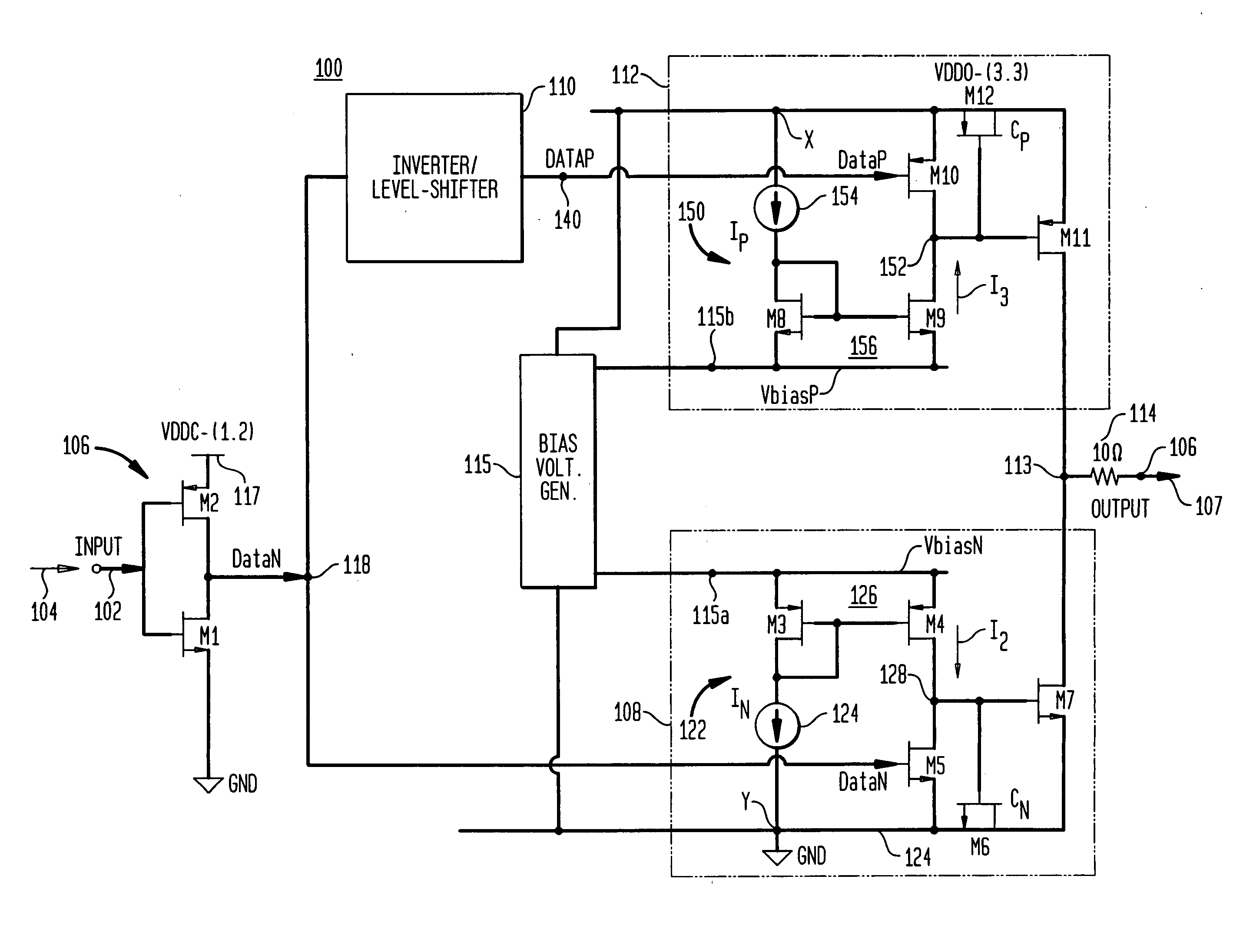
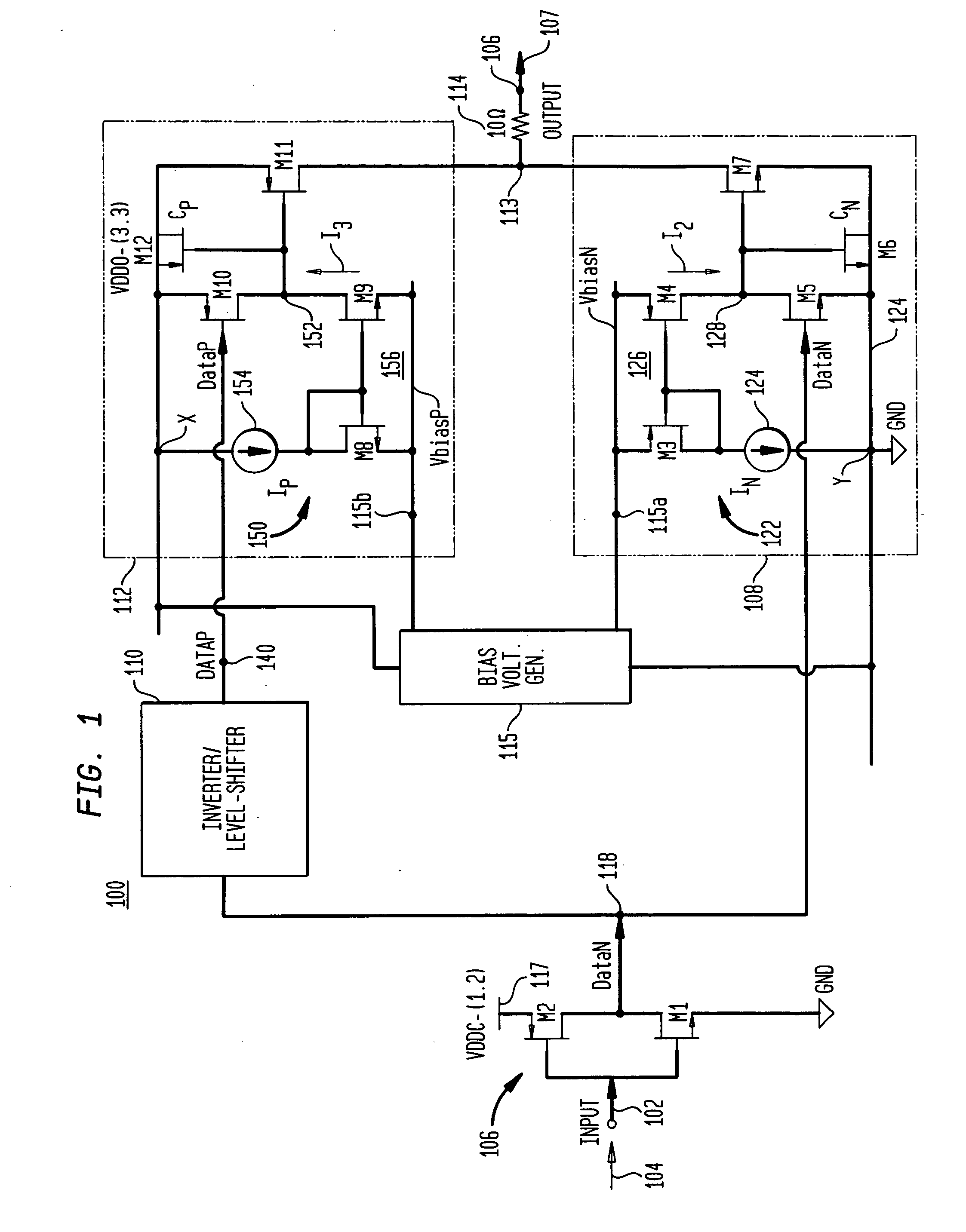
[0017] CMOS—Complementary Metal Oxide Semiconductor.

[0018] FET—Field Effect Transistor. The gate terminal, source terminal and drain terminal of a FET are referred to herein as the gate, source and drain of the FET, respectively.

[0019] NMOS—n-type MOS. In FIG. 1, an arrow pointing from the gate to the source of a FET indicates an NMOS FET, while an arrow pointing in the opposite direction indicates a PMOS FET, as is understood in the art.

[0020] PMOS—p-type MOS, which is complementary to NMOS.

Overview

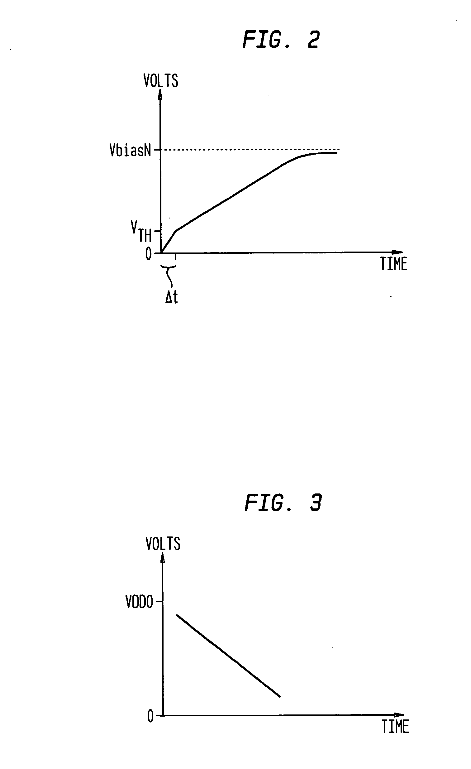
[0021]FIG. 1 is a circuit and block diagram of an example output buffer 100 constructed and operated in accordance with the present invention. Buffer 100 may be constructed on a single IC. In an embodiment, output buffer 100 is a PCI-X Input / Output (I / O) output buffer. Buffer 100 includes an input terminal 102 for receiving an input logic signal or voltage 104, an output terminal 106, and circuitry, coupled between the input and output terminals, for producing an output l...


PUM


Abstract

An output buffer includes first and second circuit portions coupled between input and output terminals. Each circuit portion includes a capacitive element; an output transistor having a gate coupled to the capacitive element, and a drain that drives a voltage at the output terminal; and a current generator configured to generate a charging current that is directed to the capacitive element responsive to a logic transition at the input terminal, wherein the charging current causes a substantially linear ramp voltage to form at the gate of the output transistor, whereby the ramp voltage controls a slew rate of the output terminal voltage.

Description

BACKGROUND [0001] 1. Field of Invention [0002] The present invention relates generally to output buffer circuits. [0003] 2. Related Art [0004] An output buffer that operates in a parallel interface, such as the Peripheral Component Interface (PCI)-X (where X indicates enhancement to PCI), is required to operate at ever increasing data rates. Typically, the output buffer is also required to drive large capacitive loads. To help meet such requirements, the output buffer needs to have an output slew rate and an output impedance that are both well controlled. [0005] With the reduced power supply voltages used on deep sub-micron CMOS Integrated Circuit (IC) chips, in addition to the increased operating speeds mentioned above, the impact of noise generated by simultaneous switched outputs of a conventional output buffer can cause spurious components that interfere with other signals on a given IC chip or on an application circuit board / card using the conventional output buffer. Thus, ther...

Claims


Application Information

Patent Timeline
Patent Type & Authority Applications(United States)
IPC IPC(8): H03K19/003
CPCH03K19/00361
Inventor VORENKAMP, PIETER
Owner AVAGO TECH WIRELESS IP SINGAPORE PTE
Why Eureka
Try Eureka