During such operation, these power devices lose energy to
self heating, both during periods of on-state conduction and during the act of switching.
These switching and conduction losses adversely limit the power converter's efficiency, potentially create the need for cooling the power devices, and in battery powered applications shorten battery life.
Using today's conventional power transistors as
power switching devices in switching
regulator circuits, an unfavorable tradeoff exists between minimizing conduction losses and minimizing switching losses.
Larger lower resistance transistors exhibit less conduction losses, but manifest higher
capacitance and increased switching losses.
Smaller devices exhibit less switching related losses but have higher resistances and increased conduction losses.
At higher switching frequencies this trade-off becomes increasingly more difficult to manage, especially for today's
power MOSFET devices, where device and converter performance and efficiency must be compromised to achieve higher frequency operation.
For alkaline and NiMH batteries the minimum voltage condition fully discharged is actually 0.9V, making it even harder to adequately switch on the
power MOSFET.
To make the MOSFET switch large enough to exhibit a low on-resistance with so little gate drive requires a very large device having large
capacitance and excessive switching losses associated with driving its gate at high frequencies.
The
disadvantage with this approach is the converter suffers lower efficiency.
Some current is lost to ground and
some energy is lost to heat.
If the gate drive current, which may be substantial, is powered from the output, the input power to the gate drive already involves additional efficiency loss (compared to powering the switch directly from the battery).
The result is that powering the MOSFET from the output is less efficient than the efficiency achievable if an ideal switch driven from a 1V input existed.
Unfortunately, conventional
silicon MOSFETs do not make good power switches in applications with only one
volt of available gate drive.
This leakage increases with decreasing threshold and increasing temperature, especially for thresholds below 0.6V, making the device unattractive as a normally-off power switch.
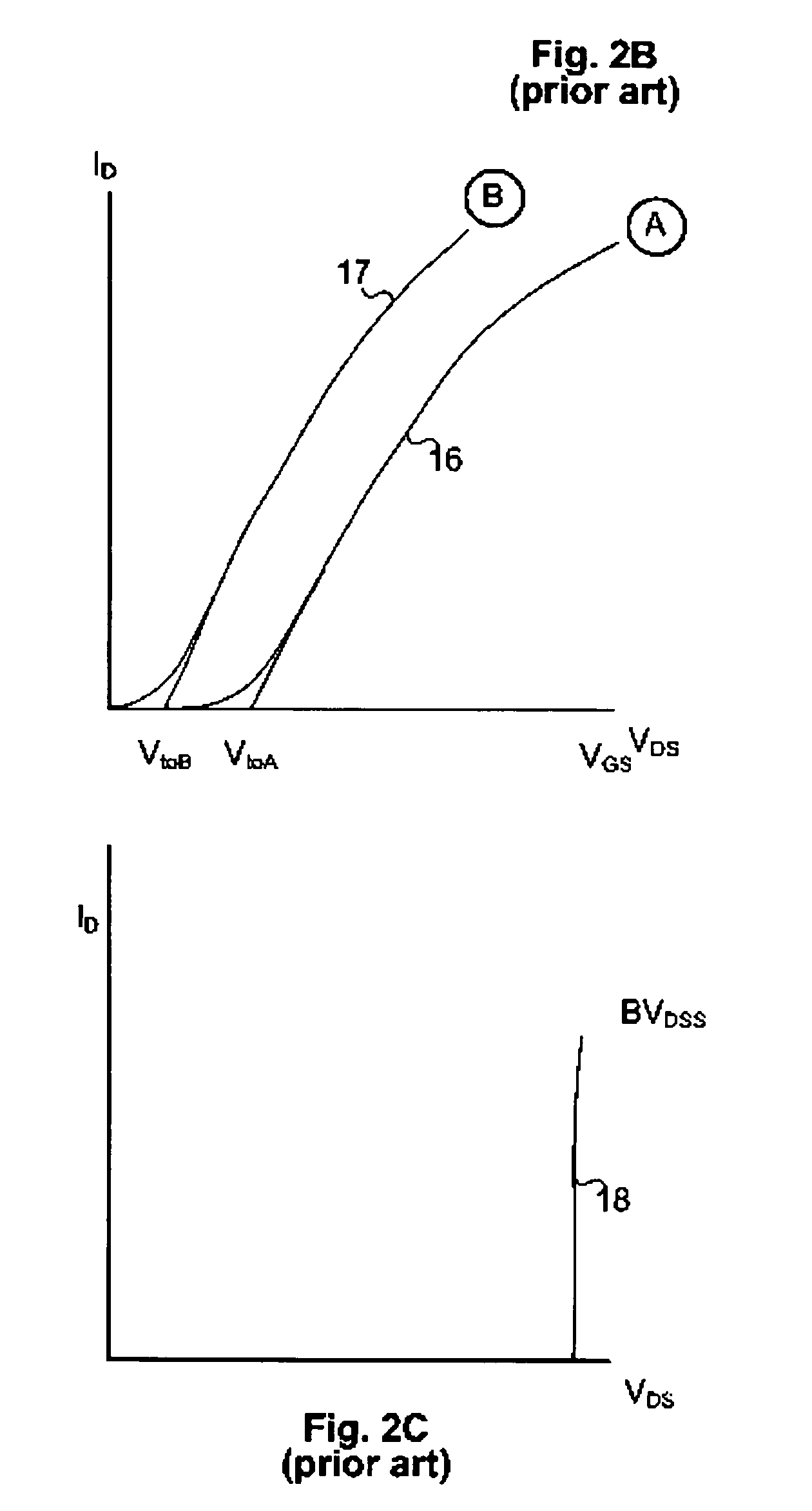
In addition to the tradeoff between leakage and on-resistance, a power MOSFET also exhibits a trade-off between its on-resistance and its switching losses.
In devices operating at voltages less than one hundred volts and especially below thirty volts, switching losses are dominated by those losses associated with driving its gate on and off, i.e. charging and discharging its input
capacitance.
Overdriving the gate to higher voltages decreases on-resistance but increases gate charge
and gate drive losses.
Inadequate gate drive leads to large increases in on-resistance, especially below or
near threshold voltage.
Minimizing the QG·RDS product of a
silicon MOSFET is difficult since changes intended to improve gate charge tend to adversely
impact on-resistance.
Historically, its limited use is due to a variety of issues including high cost, low yield, and numerous device issues including
fragility, and its inability to fabricate a MOSFET or any other insulated gate active device.
While cost and yield issues have diminished (somewhat) over the last decade, the device issues persist.
The greatest limitation in device fabrication results from its inability to form a
thermal oxide.
Without any available
dielectric, isolation between GaAs devices is also problematic, and has thwarted many commercial efforts to achieve higher levels of integration prevalent in
silicon devices and silicon integrated circuits.
Contact between the
Schottky gate and said N+ layer will result in unacceptably high gate leakage and impair the device's normal operation.
Excessive forwarding biasing of the Schottky junction at
high current densities may also permanently damage the device.
Note that the maximum extent of the
depletion region may be unable to pinch-off the
drain current totally, in which case the device cannot be fully turned off.
Such a device, where the minimum drain leakage IDmin is substantially above zero, does not make a useful power switch.
The MOSFET has much lower off-state leakage current and higher off-state resistance than the MESFET but is more costly in
power consumption to switch at high frequencies.

