

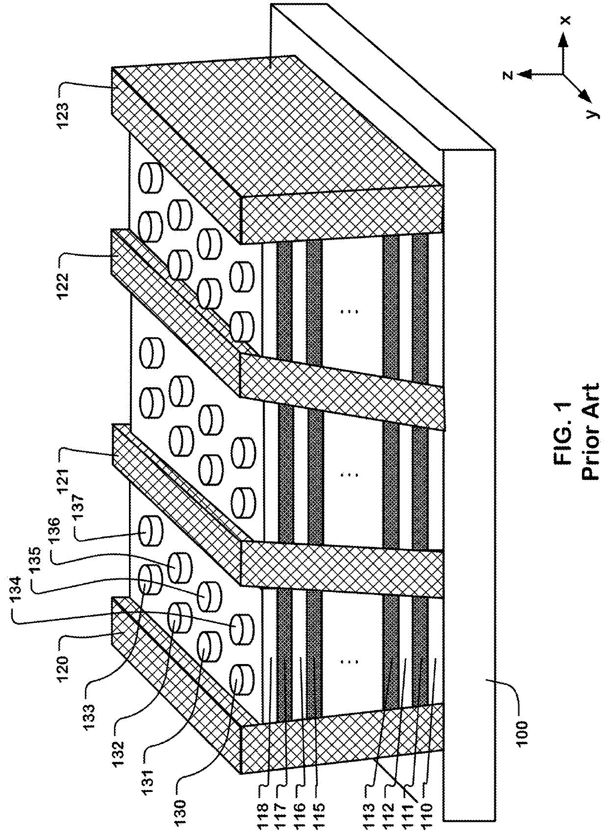
3D memory device with layered conductors
a memory device and conductor technology, applied in semiconductor devices, semiconductor/solid-state device details, electrical devices, etc., can solve problems such as difficult deformation of conductor-filled trenches, misconnection to back-end-of-line routings, and/or misalignment of beol routings, so as to reduce the stress induced deformation of the device
- Summary
- Abstract
- Description
- Claims
- Application Information
AI Technical Summary
Benefits of technology
Problems solved by technology
Method used
Image

Examples
Embodiment Construction
[0017]A detailed description of embodiments of the present invention is provided with reference to the FIGS. 2-9.
[0018]FIGS. 2 through 9 illustrate an example process flow for an integrated circuit comprising a vertical channel three-dimensional structure.
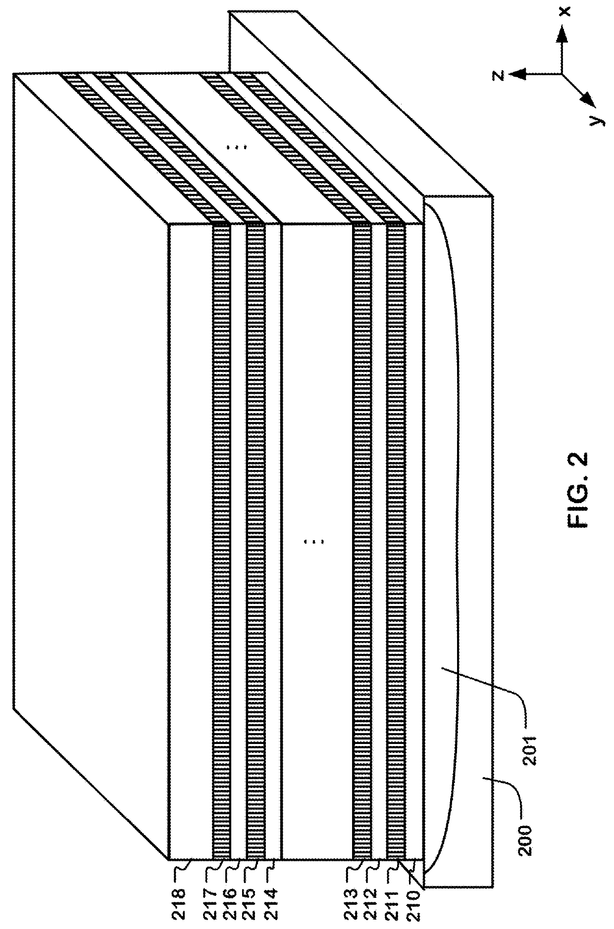
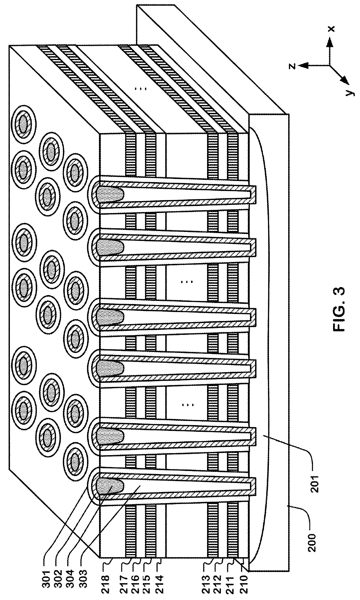
[0019]FIG. 2 is a perspective view illustrating a stage of the process after formation of a stack of active and inactive layers over a substrate 200. The term “substrate” as used herein refers to any structure below the conductor-filled trenches describe herein, and can include multiple layers including more active and inactive layers, complex structures, such as underlying circuitry, bulk semiconductor of the wafer die, and so on. The substrate 200 can be for example a bounded conductive plate formed by a doping process, in which n-type or p-type doping materials are added to a semiconductor layer or bulk semiconductor to form a conductive layer 201. Then, a stack comprising active layers (e.g. 211, 213, 215, 217), inactive layers...
PUM
 Abstract
Description
Claims
Application Information