
Integrated circuit device with layered trench conductors

a technology of integrated circuits and trenches, which is applied in the direction of semiconductor devices, semiconductor/solid-state device details, electrical apparatus, etc., can solve the problems of more likely to occur problems, difficult to form conductor-filled trenches, and more likely to be connected to back-end-of-line routings. , to achieve the effect of reducing the stress-induced deformation of the devi

Active Publication Date: 2019-08-20
MACRONIX INT CO LTD
View PDF16 Cites 3 Cited by
  • Summary
  • Abstract
  • Description
  • Claims
  • Application Information

AI Technical Summary

Benefits of technology

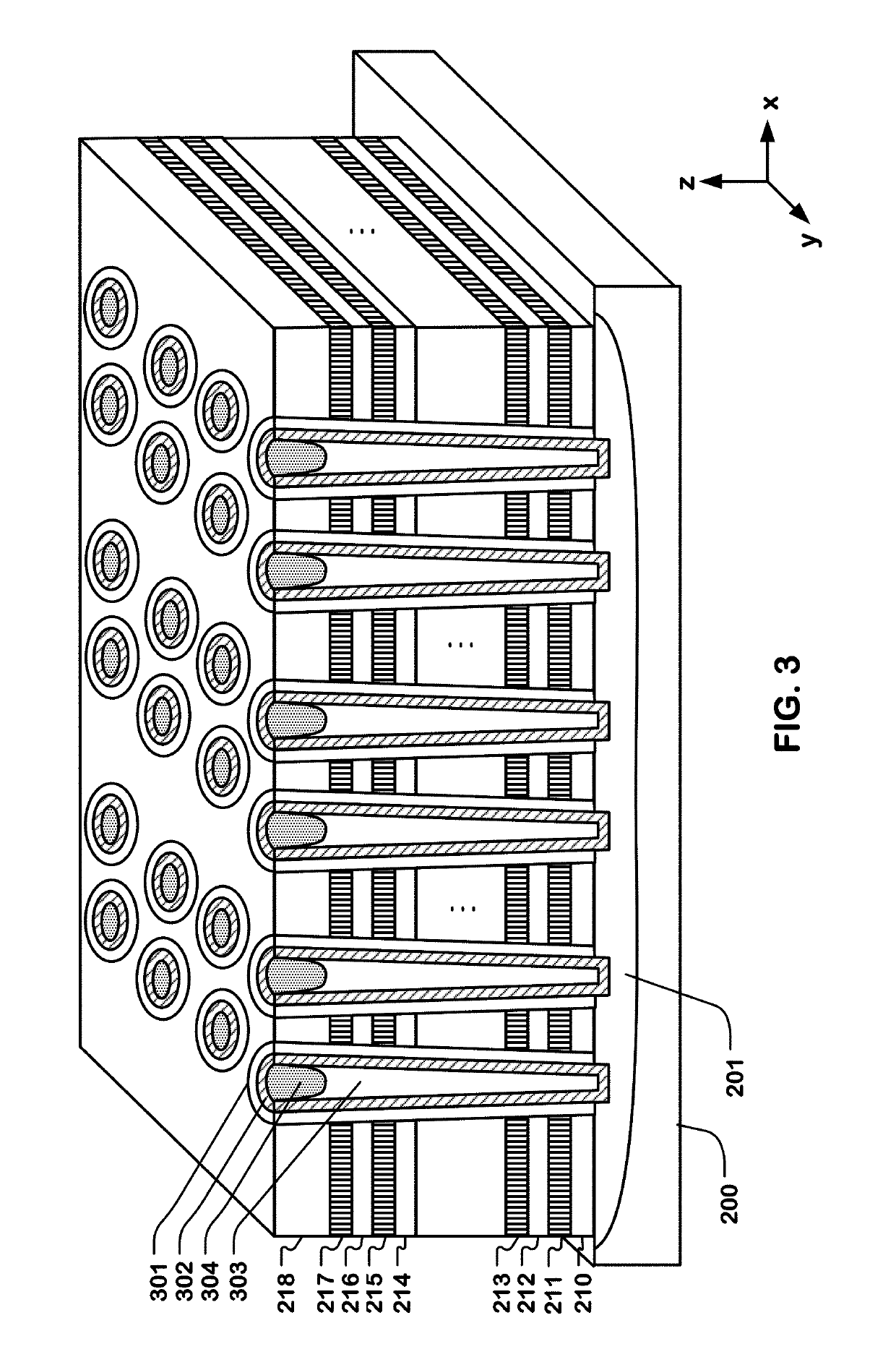
[0010]Processes for making elongated, conductor-filled trenches (i.e. trench conductors) and the resulting structures are described, which can reduce stress induced deformation of the device being formed. Thus, in one aspect, an integrated circuit described herein comprises a circuit structure, that can comprise a multilayer stack of active and inactive layers, over a substrate; a plurality of elongated trenches in the circuit structure, the elongated trenches in the plurality extending through the circuit structure to the substrate beneath the multilayer stack, and having sidewalls; and a plurality of layered trench conductors filling the corresponding elongated trenches in the plurality of elongated trenches. In embodiments described herein, a layered trench conductor in the plurality of trench layered conductors includes a bottom conductor layer in electrical contact with the substrate, a top conductor layer over the bottom conductor layer, and an intermediate dielectric or conductive layer between the top conductor layer and a portion of the sidewalls of the corresponding trench.
[0011]According to another aspect, a trench conductor in the plurality of trench conductor includes a liner conductor conformal with sidewalls of a corresponding elongated trench and in electrical contact with the substrate. A first fill body fills a lower portion of the elongated trench between the sidewalls of the corresponding elongated trench over the liner conductor. The first fill body as an upper surface recessed from the top surface of the circuit structure. A top conductor body feels an upper portion of the elongated trench between the sidewalls of the corresponding elongated trench over the liner conductor, and in current flow communication with the liner conductor. An embodiment is described in which the top conductor body includes a liner layer lining the upper portion of the corresponding elongated trench over the liner conductor and a conductive fill. The liner layer can act as an adhesion layer for improved quality of the structure at the interface between the first fill body and the top conductor body.
[0012]In an embodiment described, the fill body has a stress characteristic that is effective to compensate for stress induced by the top conductor body on the circuit structure. This can reduce or eliminate warping of the circuit structure caused by the formation of a plurality of trench conductors through it. In an example described herein, the fill body comprises a dielectric material.

Problems solved by technology

However, the formation of these conductor-filled trenches can be difficult.
This can be particularly problematic when there a multiple parallel conductors of this type being formed.
Deformation of the trenches and of devices between the trenches can present challenges of connecting the conductive lines in the stack to the backend of line (BEOL) routings.
These changes in position can cause alignment problems with upper layer structures, and lead to misconnection to and / or misalignment of back-end-of-line (BEOL) routings.
These problems are more likely to occur when the trench conductors are formed in trenches having aspect ratios of 10 or more, and depths of 1 micron or more.

Method used


Image

  • Integrated circuit device with layered trench conductors
  • Integrated circuit device with layered trench conductors
  • Integrated circuit device with layered trench conductors

Examples


Embodiment Construction

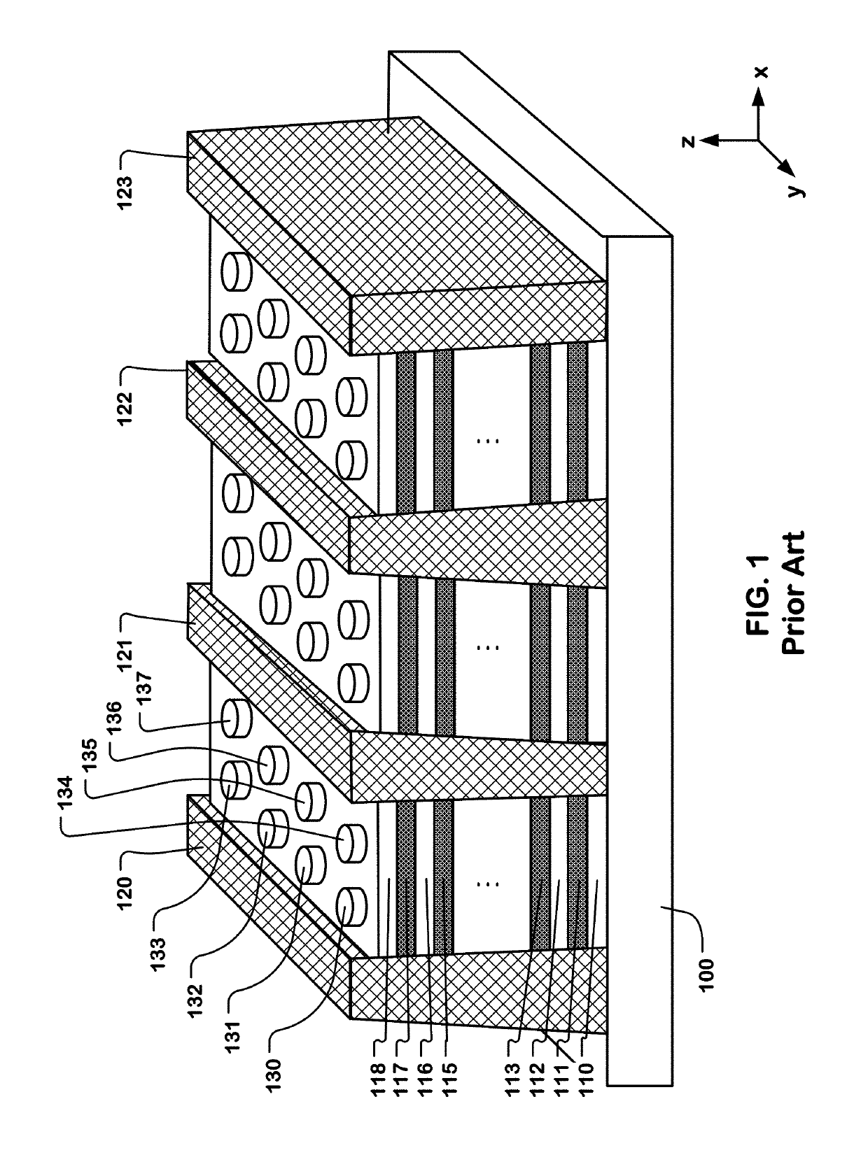
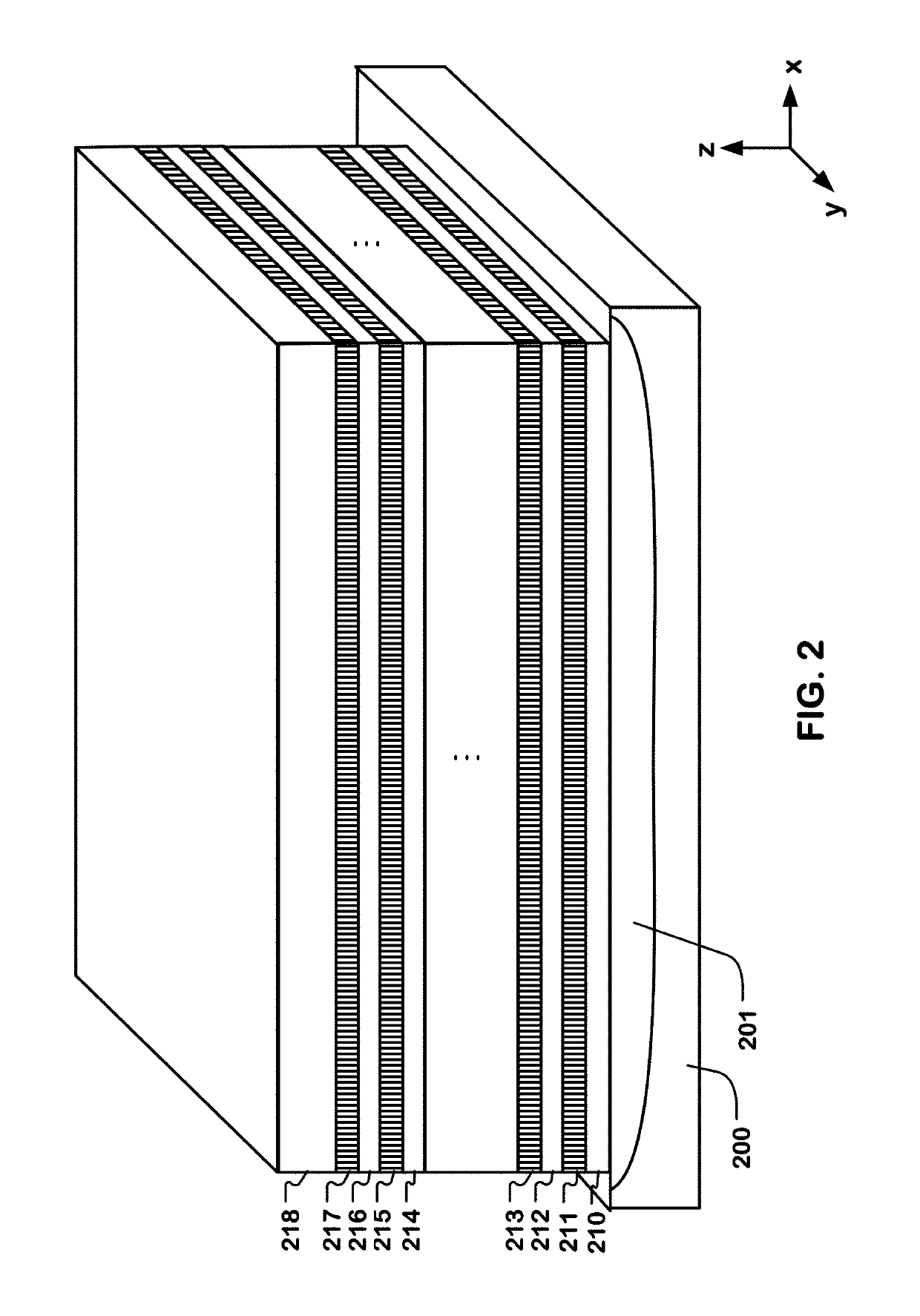
[0028]A detailed description of embodiments of the present invention is provided with reference to the FIGS. 2-16.

[0029]FIGS. 2 through 9 illustrate an example process flow for an integrated circuit comprising a vertical channel three-dimensional structure in a first embodiment.

[0030]FIG. 2 is a perspective view illustrating a stage of the process after formation of a circuit structure, which comprises in this example a stack of active and inactive layers over a substrate 200. The term “substrate” as used herein refers to any structure below the conductor-filled trenches describe herein, and can include multiple layers including more active and inactive layers, complex structures, such as underlying circuitry, bulk semiconductor of the wafer die, and so on. The substrate 200 can be for example a bounded conductive plate formed by a doping process, in which n-type or p-type doping materials are added to a semiconductor layer or bulk semiconductor to form a conductive layer 201. Then,...


PUM


Abstract

An integrated circuit includes a multilayer stack, and a plurality of layered conductors extending in the multilayer stack and into a conductor layer beneath the multilayer stack. The layered conductor has a bottom conductor layer in ohmic electrical contact with the conductive layer in a substrate, an intermediate conductive liner layer over the bottom conductor layer and lining a portion of sidewall of the corresponding trench, and a top conductor layer on the top conductive liner layer.

Description

RELATED APPLICATIONS[0001]This application is a continuation-in-part of U.S. patent application Ser. No. 15 / 462,201 filed on 17 Mar. 2017, which is incorporated by reference as if fully set forth herein.BACKGROUNDField[0002]The present technology relates to integrated circuit devices, including high density memory devices, having trench conductors.Description of Related Art[0003]Stacking multiple levels of memory cells to achieve greater storage capacity has been proposed. Researchers have been developed various structures, such as Bit Cost Scalable (BiCS) memory, Terabit Cell Array Transistor (TCAT) and Vertical NAND (V-NAND). For these types of structures, and other complex structures that comprise stacks of active layers separated by insulating (or inactive) layers, it is often useful to form conductors connecting layers deep in the stacks with upper layers or with patterned metal layers over the stacks used for connection to peripheral circuits. When these conductors require low...

Claims


Application Information

Patent Timeline
Patent Type & Authority Patents(United States)
IPC IPC(8): H01L27/11582H01L27/1157H01L23/00
CPCH01L27/11582H01L27/1157H01L23/562H10B43/27H10B43/35
Inventor HUANG, YUKAICHIANG, CHUN LINGHUNG, YUNG-TAICHENG, CHUN MINLUOH, TUUNGYANG, LING WUUYANG, TA-HUNGCHEN, KUANG-CHAO
Owner MACRONIX INT CO LTD
Learn More