Carbon Enabled Vertical Organic Light Emitting Transistors

a technology of organic light and transistor, which is applied in the direction of solid-state devices, chemistry apparatus and processes, and light-emitting compositions. it can solve the problems of poor stability, unsuitability for oled pixels, and the inability to realize the advances promised by oleds

Active Publication Date: 2018-11-08
ATOM H2O LLC
View PDF3 Cites 18 Cited by
  • Summary
  • Abstract
  • Description
  • Claims
  • Application Information

AI Technical Summary

Benefits of technology

[0049]In many other embodiments the vertical light emitting transistors further comprises a heterojunction comprising an additional carbon electrode disposed between a dielectric layer and a semiconductor layer disposed adjacent the dielectric layer of the at least one capacitor such that the vertical light emitting transistor has a two transistor and one capacitor control.
[0050]In still many other embodiments the light emitting layer

Problems solved by technology

However, the advances promised by OLEDs have not been realized at least partially as the result of limitations in the materials used in their formation.
For example, the current active matrix TFT backplanes used to drive AM-LCD pixels are typically made of amorphous silicon (a-Si), which has a low mobility (−1 cm2V−1's−1) and poor stability, and is therefore unsuitable for OLED pixels.
As a result of these deficiencies, currently AMOELD displays are driven by low temperature polycrystalline silicon (poly-Si)

Method used


Image

  • Carbon Enabled Vertical Organic Light Emitting Transistors
  • Carbon Enabled Vertical Organic Light Emitting Transistors
  • Carbon Enabled Vertical Organic Light Emitting Transistors

Examples


example 1

on of Graphene Enabled OLED

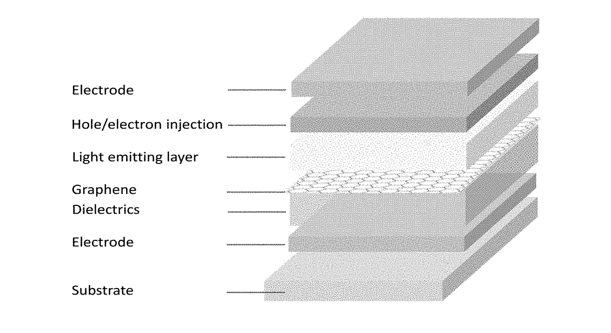
[0111]In one exemplary embodiment, shown schematically in FIGS. 1A and 1B, on substrates like glass, plastics, and silicon wafers, a layer of metal electrode (Al, Mo, Cr, Cu, Ag, Pt, Pd and Au) may be fabricated, as described, following by the fabrication of dielectrics (Al2O3, SiO2, HfO2, SiNx, ZrO2, BaSrO3, BaTiO3, polymer, polymer electrolytes, electrolytes, ionic liquids, and ionic gels), again as previously discussed. Then a layer of graphene may be placed on dielectrics by transfer, printing, or directly growth, as described in greater detail above. On the top of graphene, light-emitting materials (RGB small molecules or conjugated polymers) are fabricated by evaporating or spin-coating, as discussed above. Atop of light-emitting materials, hole / electron injection layer may then be deposited by evaporating or spin-coating, as discussed. The final metal electrode may then deposited to complete the device as previously discussed. Utilizing such combina...

example 2

ng Heterojunction VOLET and OLEDs

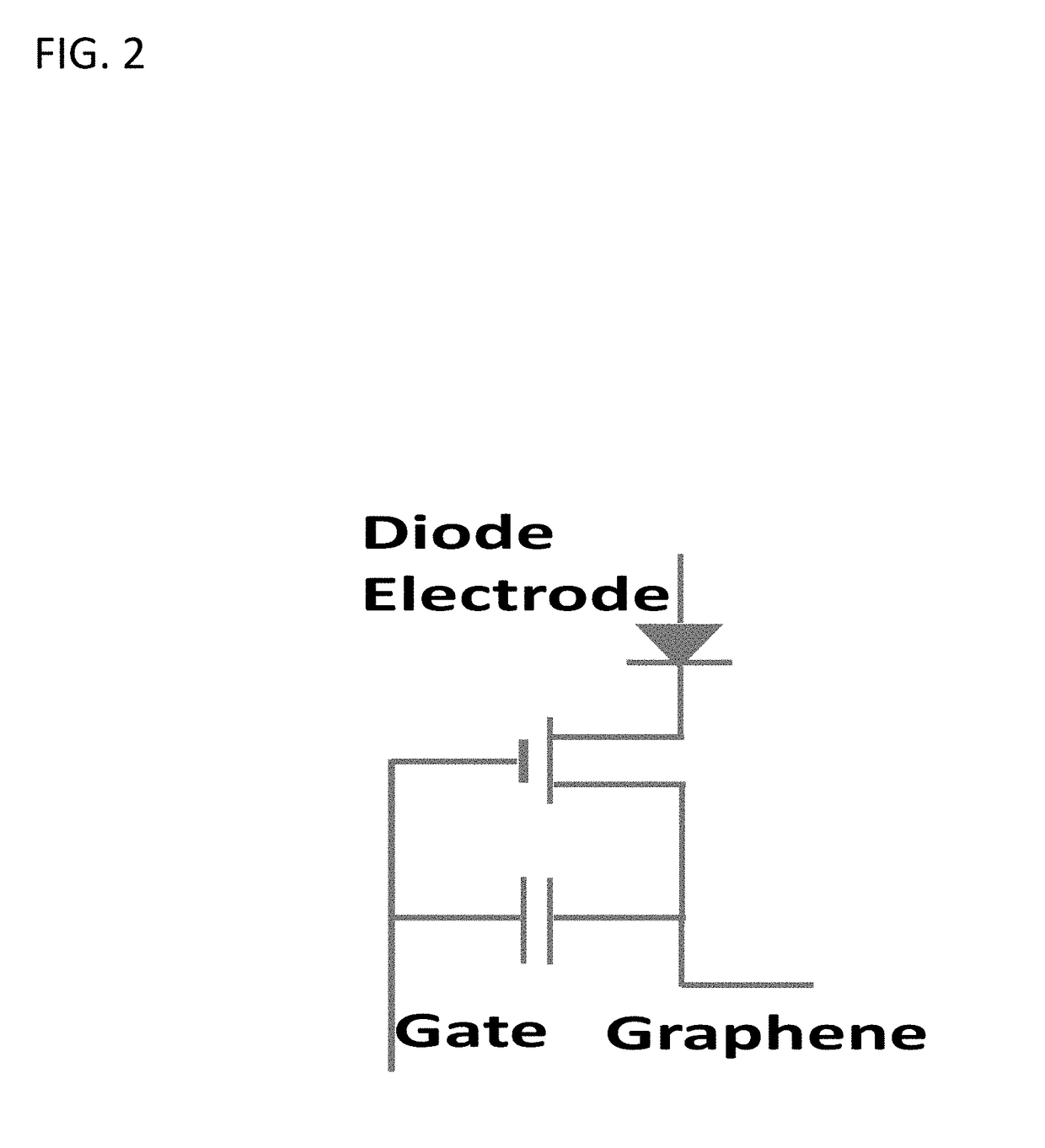
[0112]In another exemplary embodiments, shown schematically in FIGS. 4A and 4B, under bottom-gated OLED with all graphene electrodes (FIG. 3A), a graphene enabled vertical heterojunction transistor is added (FIG. 4A). The graphene enabled vertical heterojunction transistor may be built with a graphene electrode, dielectrics layer, a graphene electrode and semiconductor stacked in sequence from bottom to top, where the OLED is bottom-controlled by two transistors and one capacitor (2T1C) circuitry. Similarly, on top-gated OLED with all graphene electrodes (FIG. 3B), a graphene enabled vertical heterojunction transistor is added (FIG. 4B), where the graphene enabled vertical heterojunction transistor was built with a graphene electrode, dielectrics layer, a graphene electrode and semiconductor stacked in sequence from top to bottom. Here, OLED is top-controlled by 2T1C circuitry.

example 3

plays

[0113]Finally, although the above exemplary embodiments and discussion has focused on methods, architectures and structures for individual devices, it will be understood that the same architectures and structures may be combined as pixels into a VOLET display device. In such an embodiment, a plurality of VOLETs as described herein may be combined and interconnected as is well-known by those skilled in the art, such as by electronically coupling the VOLETs into addressing electrode lines, to form a TFT-backplane for a display, such as an AMOLED display.


PUM


Abstract

Devices, structures, materials and methods for carbon enabled vertical light emitting transistors (VLETs) and light emitting displays (LEDs) are provided. In particular, architectures for vertical polymer light emitting transistors (VPLETs) for active matrix organic light emitting displays (AMOLEDs) and AMOLEDs incorporating such VPLETs are described. Carbon electrodes (such as from graphene) alone or in combination with conjugated light emitting polymers (LEPs) and dielectric materials are utilized in forming organic light emitting transistors (OLETs). Combinations of thin films of ionic gels, LEDs, carbon electrodes and relevant substrates and gates are utilized to construct LETs, including heterojunction VOLETs.

Description

CROSS-REFERENCE TO RELATED APPLICATIONS[0001]This application claims priority to U.S. Provisional Patent Application No. 62 / 501,617, filed May 4, 2017, the disclosure of which is incorporated herein by reference.FIELD OF THE INVENTION[0002]Devices, structures, materials and methods for carbon enabled vertical organic light emitting transistors and light emitting displays are presented.BACKGROUND OF THE INVENTION[0003]Organic Light Emitting Diode (OLED) displays have been highly anticipated by electronic consumers due to their well-recognized advantages in power consumption, pixel brightness, viewing angle, response time, and contrast ratio over liquid crystal displays (LCD). (See, e.g., G. Gu and S. R. Forrest, IEEE Journal of Selected Topics in Quantum Electronics, vol. 4, pp. 83-99, 1998, the disclosure of which is incorporated herein by reference.) However, the advances promised by OLEDs have not been realized at least partially as the result of limitations in the materials used ...

Claims


Application Information

Patent Timeline
IPC IPC(8): H01L51/52H01L51/00H01L51/05H01L51/56H01L51/10H01L51/50
CPCH01L51/5296H01L51/0045H01L51/057H01L51/5206H01L51/5221H01L51/0525H01L51/56H01L51/105H01L51/5092H01L51/5012C09K11/06H10K10/491H10K10/84H10K50/81H10K50/82H10K50/30H10K10/472H10K50/11H10K50/171H10K71/00H10K85/20
Inventor LI, HUAPING
Owner ATOM H2O LLC
Why Eureka
Try Eureka