Optical waveguide device
- Summary
- Abstract
- Description
- Claims
- Application Information
AI Technical Summary
Benefits of technology
Problems solved by technology
Method used
Image
Examples
first embodiment
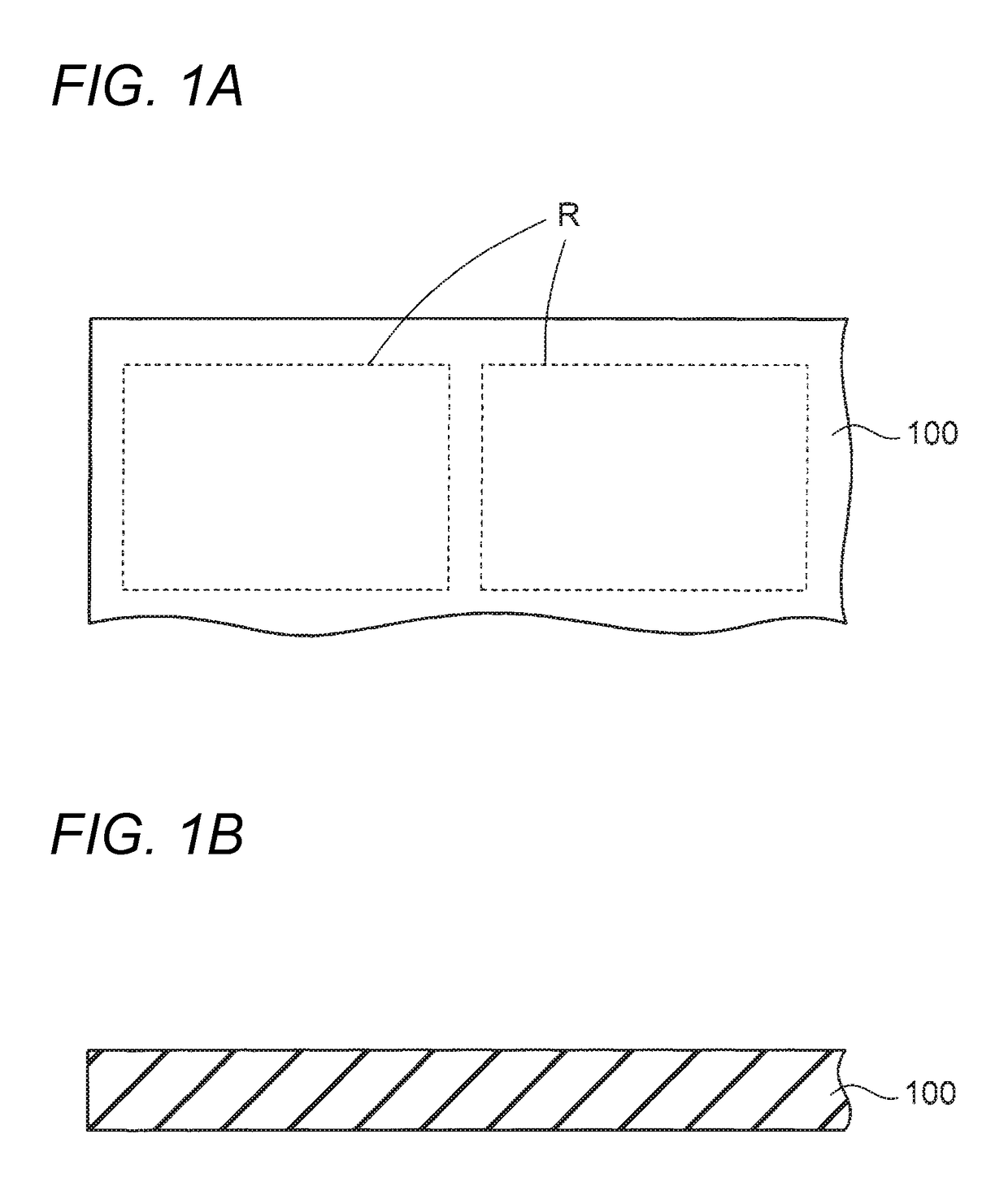
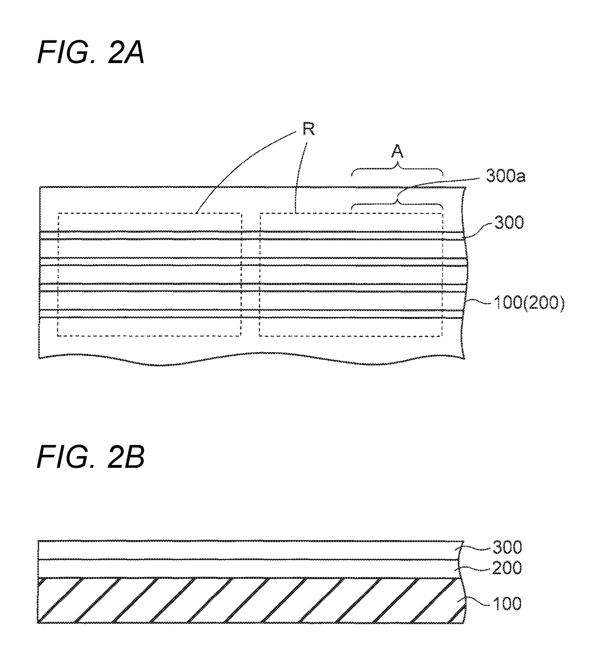
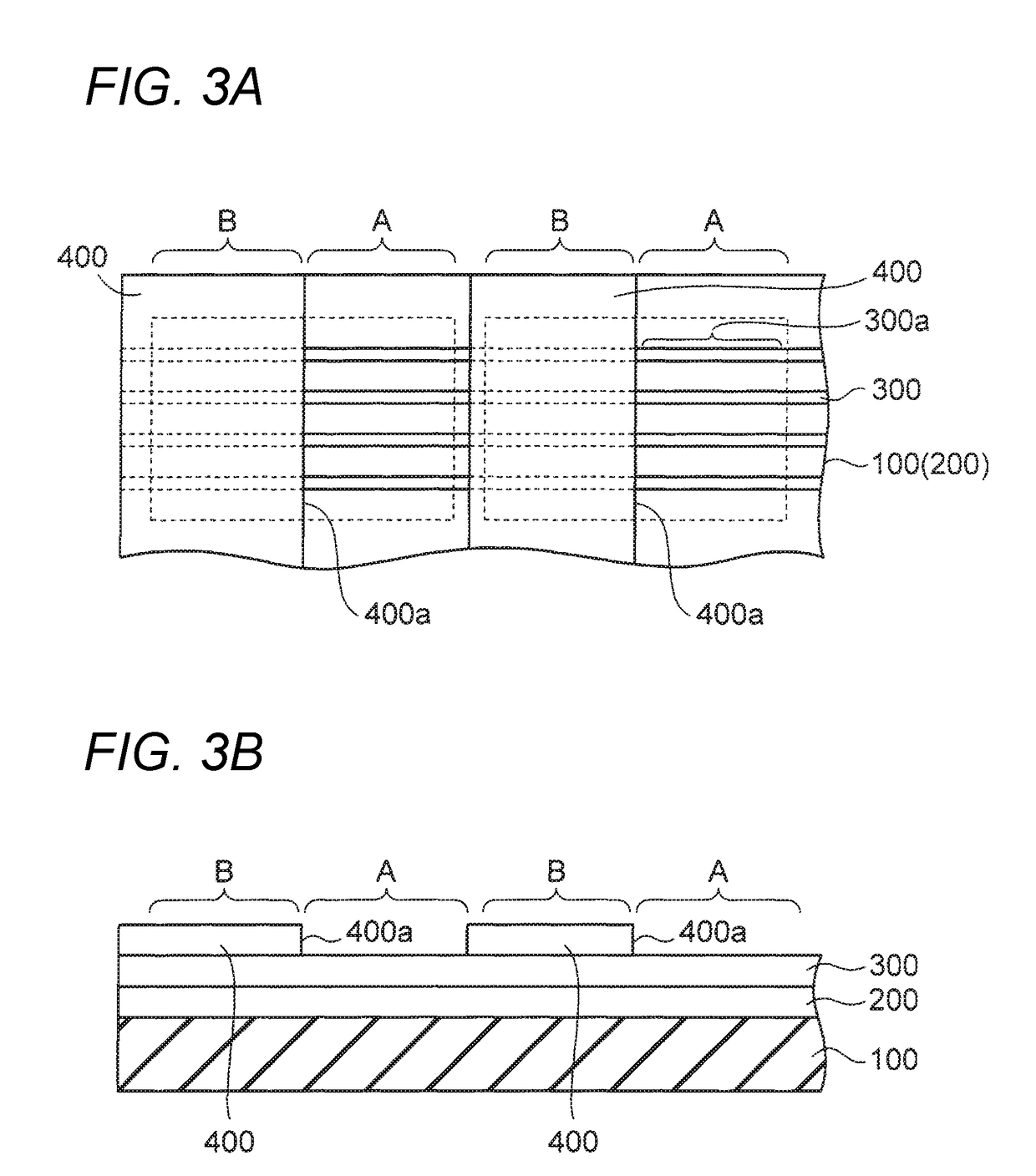
[0050]FIG. 6 to FIG. 13B are views showing a manufacturing method of an optical waveguide device according to a first embodiment. FIGS. 14A to 14D are views showing the optical waveguide device according to the first embodiment. A structure of the optical waveguide device will be described below while the manufacturing method of the optical waveguide device is described.
[0051]In the manufacturing method of the optical waveguide device according to the first embodiment, first, a substrate 10 is prepared, as shown in FIG. 6. For example, the substrate 10 is formed out of an insulating resin material such as a glass epoxy resin. The substrate 10 may be a rigid substrate high in rigidity, or a flexible substrate low in rigidity. The substrate 10 includes an insulating material called a support or a base.
[0052]As having been described in the aforementioned preliminary matter, the substrate 10 is a large-sized substrate in which a plurality of product regions R are defined in order to obt...
second embodiment
[0118]FIG. 17A to FIG. 20 are views showing a manufacturing method of an optical waveguide device according to a second embodiment. FIGS. 21A and 21B are views showing the optical waveguide device according to the second embodiment.
[0119]In the second embodiment, detailed description about the same steps and the same elements as those in the first embodiment will be omitted.
[0120]In the optical waveguide device according to the second embodiment, entire core layers of an optical waveguide serve as optical coupling portions. The entire core layers are covered with a protective layer which is formed in a removable state.
[0121]As shown in FIGS. 17A and 17B, first, the same steps as the steps of FIGS. 7A to 9B in the aforementioned first embodiment are performed. Thus, the same structure assembly as that in FIGS. 9A and 9B can be obtained. In FIGS. 17A and 17B, a first clad layer 20 and core layers 22 are formed on a substrate 10.
[0122]In FIGS. 17A and 17B, one of product regions R in t...
PUM
 Abstract
Description
Claims
Application Information


