Insulating magnetic components on silicon using pnp or npn junctions

a technology of magnetic components and junctions, which is applied in the direction of semiconductor devices, semiconductor/solid-state device details, inductances, etc., can solve the problems of limiting the compactness of magnetic components, challenging to maintain the minimum creepage and clearance distance in miniaturized constructions, and reducing the level of leakage current. , to achieve the effect of obtaining safety approval and compliance, improving compactness, and reducing the number of components

Active Publication Date: 2018-12-06
MURATA MFG CO LTD
View PDF5 Cites 0 Cited by
  • Summary
  • Abstract
  • Description
  • Claims
  • Application Information

AI Technical Summary

Benefits of technology

The present invention provides a way to insulate current conductors with a reversed biased PN junction that allows for closer proximity between the conductors while maintaining reliable dielectric strength. This results in a significantly lower level of leakage current that makes it easier to achieve safety approval and compliance with regulations. By using insulation with PN junctions, the invention improves compactness and reduces the thickness of the insulation. This is important because it allows for closer proximity between the current conductors.

Problems solved by technology

One of the reasons for not being able to miniaturize magnetic components in proportion to the increase in operating frequencies is the difficulty of maintaining the dielectric strength between the turns of a single winding (inter-turn dielectric strength) and between the primary and secondary windings (inter-winding dielectric strength).
It is also challenging to maintain the minimum creepage and clearance distances in miniaturized constructions.
As the magnetic components become more compact, it becomes more challenging to meet the isolation requirement between separate windings and between turns of a single winding, which limits how compact magnetic components can be.
This is a considerable constraint in achieving highly compact magnetic components, especially in the case of low-power applications, such as magnetic components formed in silicon.
But the oxidized semiconductor layer does not provide adequate dielectric strength, which can result in inadequate isolation properties.

Method used


Image

  • Insulating magnetic components on silicon using pnp or npn junctions
  • Insulating magnetic components on silicon using pnp or npn junctions
  • Insulating magnetic components on silicon using pnp or npn junctions

Examples


Embodiment Construction

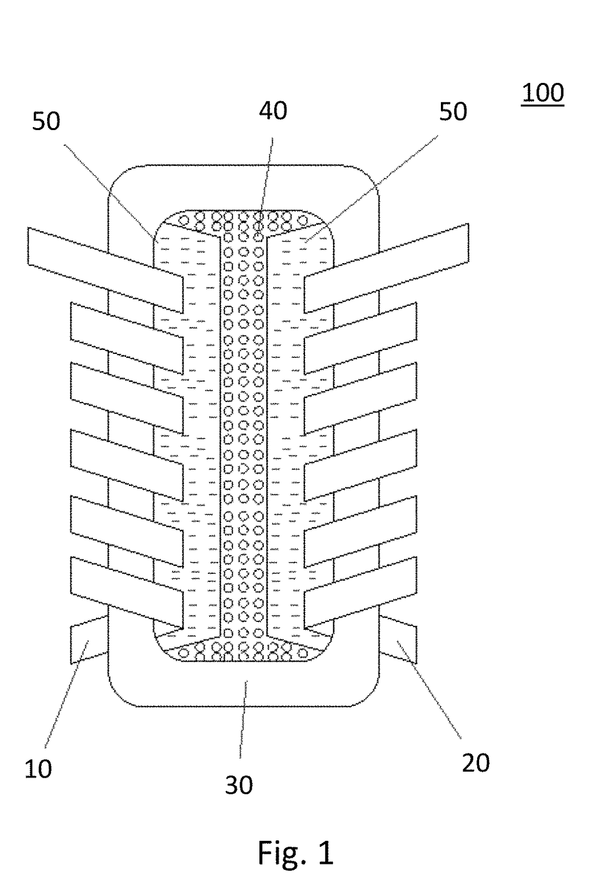
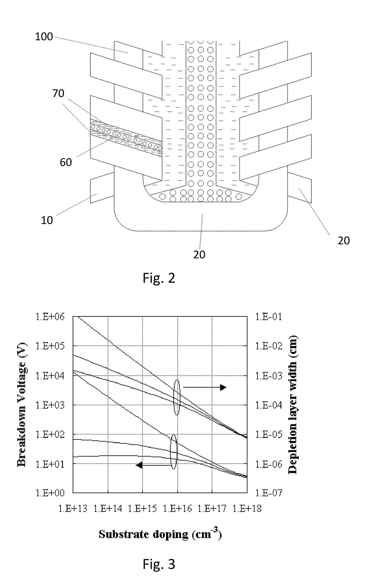
[0027]Insulation including two NP junctions, which will be referred to as NPN-junction insulation, is shown in FIGS. 1, 2, and 4. FIG. 1 shows a transformer 100 with inter-winding insulation between two windings 10, 20. FIG. 2 shows a transformer 100 with both inter-winding insulation between two windings 10, 20 and intra-winding insulation between the turns of one of the windings 10. For simplicity, in FIG. 2, intra-winding insulation is only shown between two adjacent turns in one of the windings 10. Intra-winding insulation can be used between every pair of adjacent turns in both windings 10, 20. FIG. 4 shows a transformer 100 with inter-winding insulation between two windings 10, 20. The transformers 100 in FIGS. 1 and 4 can also include intra-winding insulation between the turns of each of the windings 10, 20.

[0028]Inter-winding insulation includes the NPN-junction defined by a P-doped region 40 and an N-doped region 50, and intra-winding insulation includes the NPN-junction de...


PUM


Abstract

A magnetic component includes a semiconductor substrate, a first winding that is located in the semiconductor substrate and that includes at least two turns, and intra-winding insulation located between two adjacent turns of the at least two turns and including doped regions in the semiconductor substrate that define either an NPN-junction or a PNP junction.

Description

BACKGROUND OF THE INVENTION1. Field of the Invention[0001]The present invention relates to using PNP or NPN (PNP / NPN) junctions to provide insulation of magnetic components, including magnetic components formed on silicon such as micro-transformers, micro-inductors, and other compact magnetics such as PCB-integrated magnetic components.2. Description of the Related Art[0002]There is an increasing demand for smaller and smaller magnetic components. Typically, as the operating frequencies increase, the magnetic components get smaller, but this is not always true or it does not happen in proportion to the increase in frequency. One of the reasons for not being able to miniaturize magnetic components in proportion to the increase in operating frequencies is the difficulty of maintaining the dielectric strength between the turns of a single winding (inter-turn dielectric strength) and between the primary and secondary windings (inter-winding dielectric strength). It is also challenging t...

Claims


Application Information

Patent Timeline
Patent Type & Authority Applications(United States)
IPC IPC(8): H01L49/02H01L29/06H01L21/761H10N97/00
CPCH01L28/10H01L29/0646H01L21/761H01L2924/3011H01L23/645
Inventor WARNAKULASURIYA, KAPILA
Owner MURATA MFG CO LTD
Why Eureka
Try Eureka