
Image sensor, image-capturing apparatus, and semiconductor memory

a technology which is applied in the field of image sensor and image capture apparatus, can solve the problem that the image sensor cannot increase the speed of reading out signals from the pixels, and achieve the effect of improving the reading speed of images

Inactive Publication Date: 2019-04-11
NIKON CORP
View PDF8 Cites 0 Cited by
  • Summary
  • Abstract
  • Description
  • Claims
  • Application Information

AI Technical Summary

Benefits of technology

This patent is related to an image sensor that can capture images. The invention focuses on improving the sensor's performance by reducing the time required for image processing. The patent proposes a method for adjusting the timing between different components of the image sensor, including the first circuit, the readout unit, and the amplifying unit. By controlling these timings, the image sensor can operate more efficiently and quickly, resulting in better image quality and reduced latency.

Problems solved by technology

Such an image sensor cannot increase a speed of reading out signals from the pixels when the number of pixels increases.

Method used


Image

  • Image sensor, image-capturing apparatus, and semiconductor memory
  • Image sensor, image-capturing apparatus, and semiconductor memory
  • Image sensor, image-capturing apparatus, and semiconductor memory

Examples


first embodiment

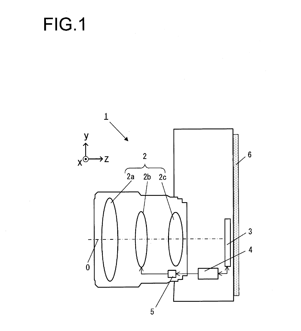
[0048]FIG. 1 is a cross-sectional view schematically illustrating a configuration of an image-capturing apparatus using an image sensor according to a first embodiment. The image-capturing apparatus 1 includes an image-capturing optical system 2, an image sensor 3, a control unit 4, a lens driving unit 5, and a display unit 6.

[0049]The image-capturing optical system 2 forms a subject image on an image-capturing surface of the image sensor 3. The image-capturing optical system 2 includes a lens 2a, a focusing lens 2b, and a lens 2c. The focusing lens 2b is a lens for performing focal adjustment of the image-capturing optical system 2. The focusing lens 2b is capable of being driven in an optical axis O direction.

[0050]The lens driving unit 5 has an actuator (not illustrated). Using the actuator, the lens driving unit 5 drives the focusing lens 2b by a desired amount in the optical axis O direction. The image sensor 3 captures the subject image and outputs an image. The control unit 4...

first modification

(First Modification)

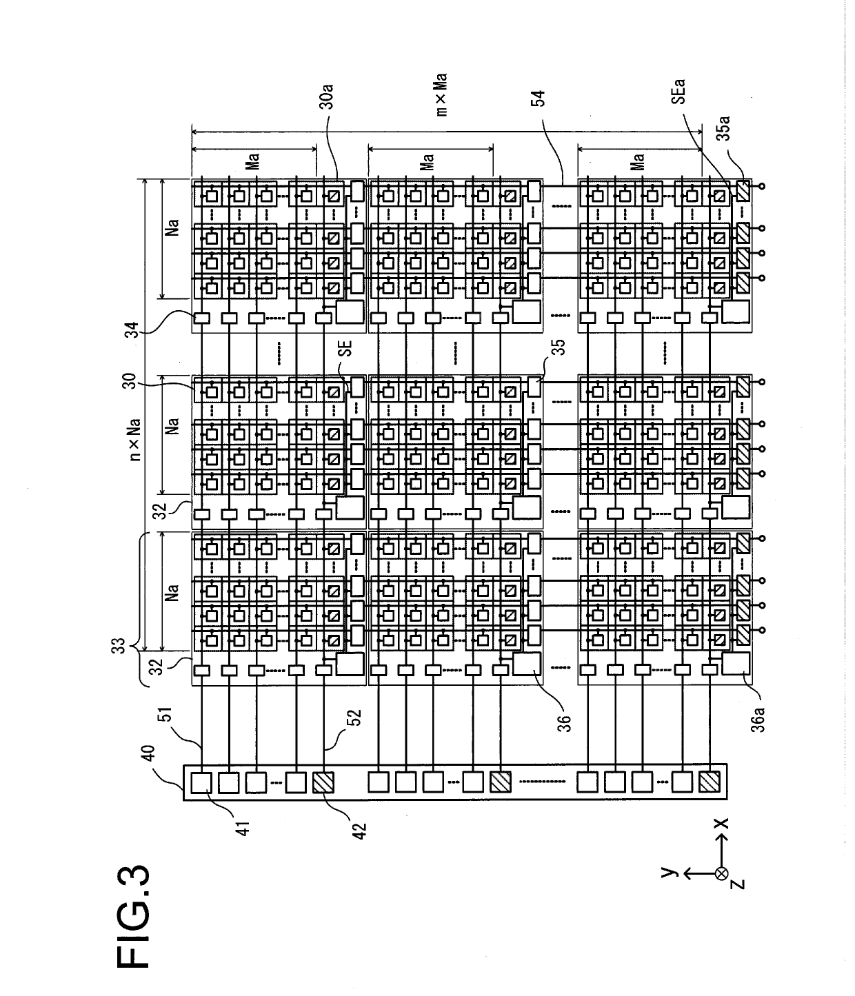
[0141]The pixel block column 33 may be configured to include one pixel block 32 instead of the plurality of pixel blocks 32. In other words, the relay amplifier circuit 35, the relay amplifier control circuit 36, the relay signal output unit 42, and the like are not necessarily provided.

[0142]While various embodiments and modifications have been described above, the present invention is not limited thereto. Other embodiments contemplated within the technical idea of the present invention are also included within the scope of the present invention.

[0143]The disclosure of the following priority application is herein incorporated by reference:

[0144]Japanese Patent Application No. 2016-69737 (filed Mar. 30, 2016)


PUM


Abstract

A first circuit constituting a plurality of first circuit in a first direction, which stores a signal output from a pixel having a photoelectric conversion unit; a first control unit to which the plurality of first circuits are connected and outputs a first signal for outputting signals stored in the plurality of first circuits; a readout unit that reads out the signal output from the first circuit; a plurality of second circuits that are connected to the first control unit, a plurality of sets of the plurality of second circuits in the first direction; and a second control unit that controls a readout of the signal by the readout unit. The first control unit outputs a second signal to the plurality of second circuits together with the first signal; and the second control unit controls the readout of the signal by the readout unit, based on the second signal.

Description

TECHNICAL FIELD[0001]The present invention relates to an image sensor, an image-capturing apparatus, and a semiconductor memory.BACKGROUND ART[0002]PTL1 discloses an image sensor in which chips having pixels formed thereon and chips having pixel driving circuits formed thereon are stacked on each other, the pixel driving circuits driving the pixels. Such an image sensor cannot increase a speed of reading out signals from the pixels when the number of pixels increases.CITATION LISTPatent Literature[0003]PTL1: Japanese Laid-Open Patent Publication No. 2010-225927SUMMARY OF INVENTION[0004]According to the 1st aspect of the present invention, an image sensor comprises: a first circuit constituting a plurality of first circuits provided in a first direction, which stores a signal output from a pixel having a photoelectric conversion unit; a first control unit to which the plurality of first circuits are connected and which outputs a first signal for outputting signals stored in the plura...

Claims


Application Information

Patent Timeline
Patent Type & Authority Applications(United States)
IPC IPC(8): H04N5/378H01L27/146H04N5/3745
CPCH04N5/378H01L27/14634H04N5/37457H01L27/1464H04N23/50H04N25/78H01L27/146H04N25/778H04N25/771H04N25/79H04N25/75
Inventor KOMAI, ATSUSHI
Owner NIKON CORP
Learn More