

Liquid crystal display with in-cell phase difference layer
a phase difference layer and liquid crystal display technology, applied in the field of liquid crystal display, can solve the problems of deteriorating display characteristics, low photo efficiency, and deteriorating and achieve the effect of improving display characteristics and increasing the contrast ratio of lcd
Active Publication Date: 2019-04-18
SAMSUNG ELECTRONICS CO LTD
View PDF3 Cites 0 Cited by
- Summary
- Abstract
- Description
- Claims
- Application Information
AI Technical Summary
Benefits of technology
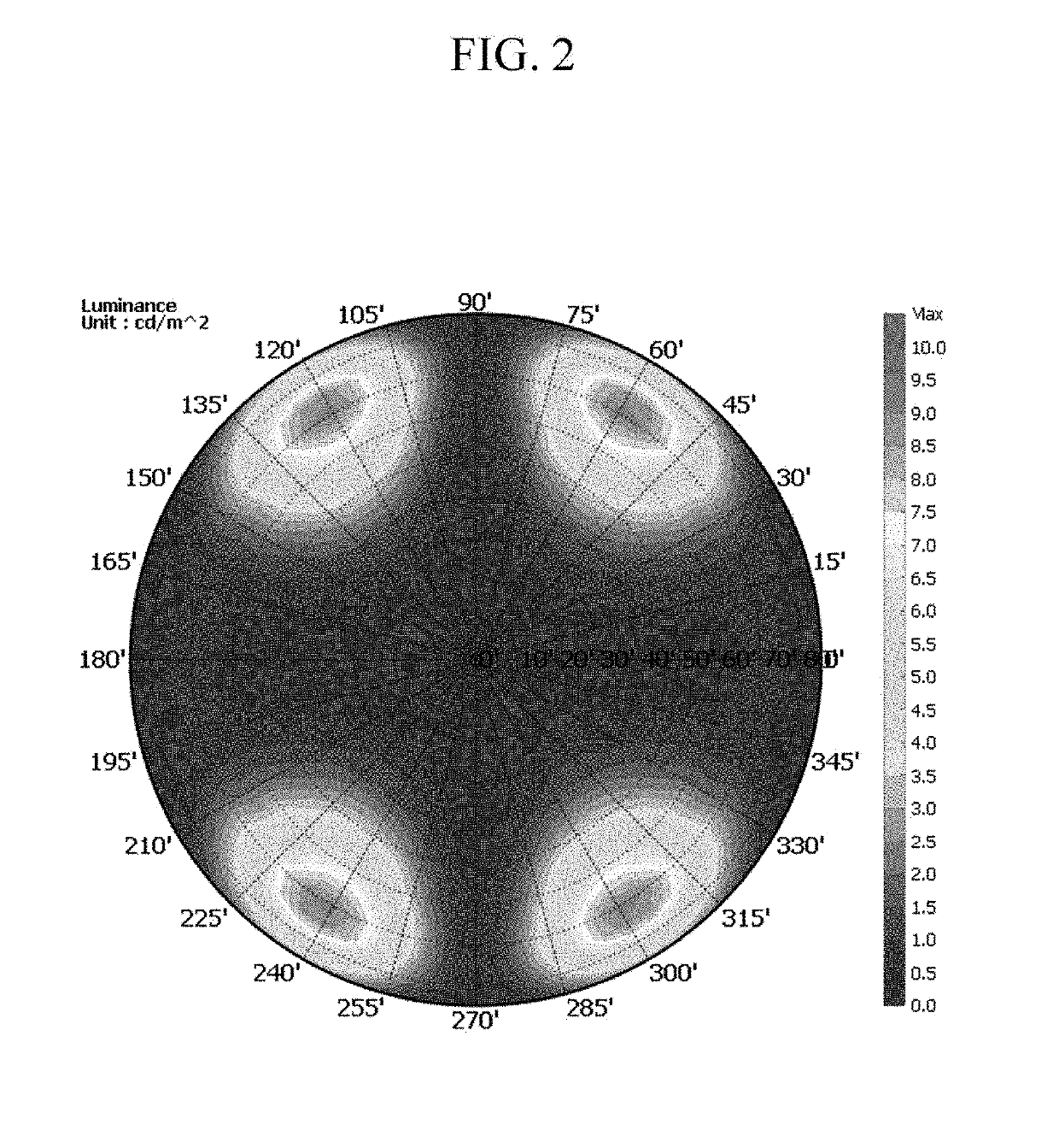
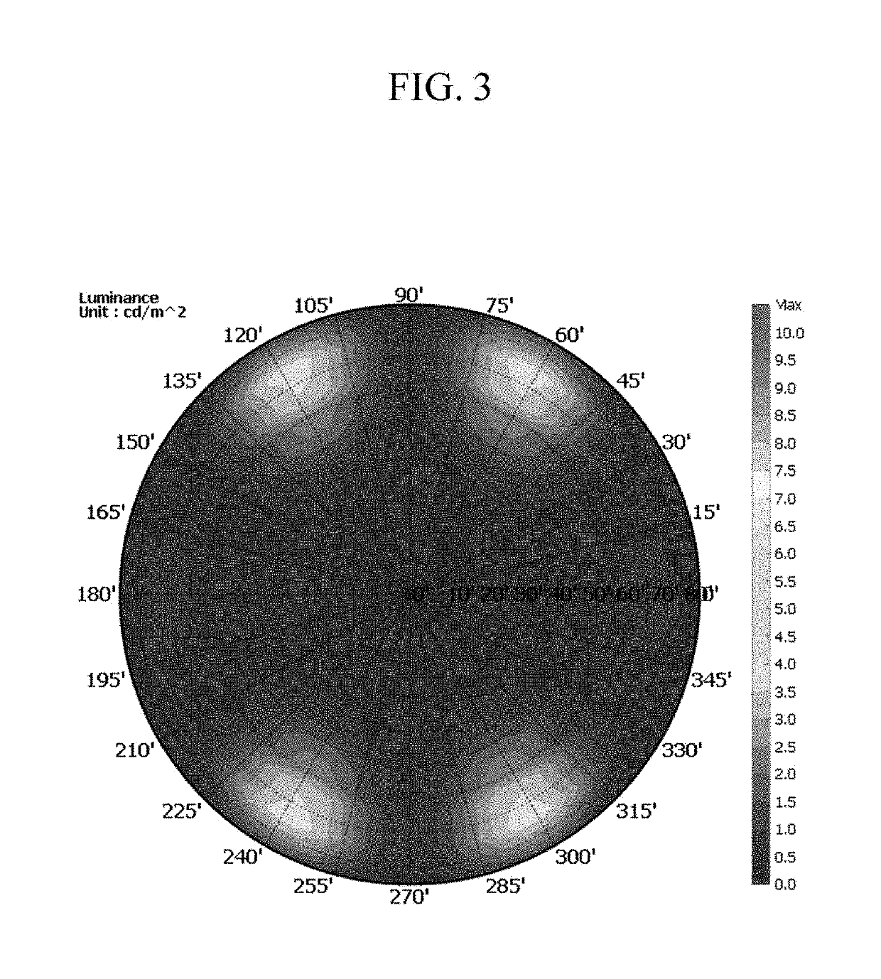
[0057]In an embodiment, a contrast ratio of the LCD may be
Problems solved by technology
However, a color filter absorbs a lot of light emitted from a light source, and thus lowers photo-efficiency.
However, the photo-luminescent LCD may rarely adopt a conventional structure of disposing a polarizing plate on the light emitting eleme
Method used
View moreImage
Smart ImageViewing Examples

Examples
 PUM
 Abstract
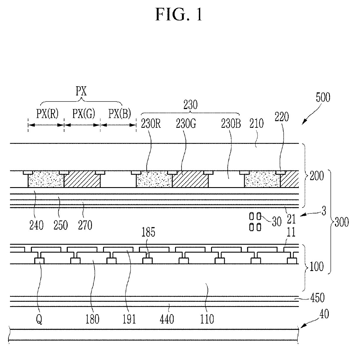
A liquid crystal display includes a lower substrate and an upper substrate facing each other, a liquid crystal layer disposed between the lower substrate and the upper substrate, a color conversion layer disposed on the liquid crystal layer, a first polarizing layer and a first phase difference layer disposed between the liquid crystal layer and the color conversion layer, and a second polarizing layer and a second phase difference layer disposed between a light source and the lower substrate, wherein the first phase difference layer has a refractive index satisfying Inequality 1 and the second phase difference layer has refractive indexes satisfying Inequality 2.
nx1≥ny1>nz1 [Inequality 1]
nx2>nz2>ny2 [Inequality 2]
In Inequalities 1 and 2, nx1, nx2, ny1, ny2, nz1, and nz2 are the same in the detailed description.
Description
CROSS-REFERENCE TO RELATED APPLICATION[0001]This application claims priority to Korean Patent Application No. 10-2017-0134030, filed on Oct. 16, 2017, and all the benefits accruing therefrom under 35 U.S.C. § 119, the content of which in its entirety is herein incorporated by reference.BACKGROUND1. Field[0002]Embodiments of a liquid crystal display are disclosed.2. Description of the Related Art[0003]A liquid crystal display (“LCD”) is one of the most widely used types of a flat panel display. The LCD generally includes two display panels formed with at least two field generating electrodes and a liquid crystal layer interposed therebetween, and liquid crystal molecules are rotated depending upon an electric field formed between the field generating electrodes to thereby vary light transmittance to display an image.[0004]The LCD displays color by combining light from a light source with a color filter. However, a color filter absorbs a lot of light emitted from a light source, and t...
Claims
Login to View More Application Information
Patent Timeline
 IPC IPC(8): G02F1/137G02F1/1337G02F1/1335G02F1/1362G02F1/1368H01L27/12
CPCG02F1/137G02F1/1337G02F1/133512G02F1/136286G02F1/1368H01L27/124G02F1/133528G02F1/133514G02F2201/123G02F2201/121G02F2001/133548G02F2001/13712G02F1/133617G02F1/133634G02F2413/02G02F1/133637G02F1/13712G02F1/133509G02F1/133548
InventorKIM, BEOM SEOKGAM, SANGAHKIM, JU HYUNCHOI, HYUN-SEOK
OwnerSAMSUNG ELECTRONICS CO LTD