Lead structure of circuit

Active Publication Date: 2019-04-18
SITRONIX TECH CORP
View PDF1 Cites 0 Cited by
  • Summary
  • Abstract
  • Description
  • Claims
  • Application Information

AI Technical Summary

Benefits of technology

[0004]An objective of the present invention is to provide a lead structure of the circuit, which adopts a necking design to increase the gap between adjacen

Problems solved by technology

Unfortunately, since the gaps between adjacent leads are narrow, it is difficult for etchants to enter.
Consequently, etching is difficult, or even the lea

Method used


Image

  • Lead structure of circuit
  • Lead structure of circuit
  • Lead structure of circuit

Examples


first embodiment

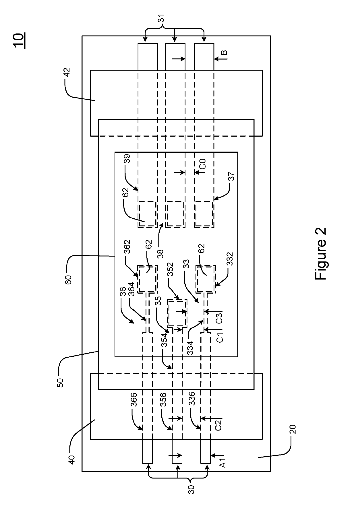
[0021]Please refer to FIG. 2, which shows a top view of the lead structure of the circuit according to the present invention applied to the chip on film package. To illustrate clearly the difference between the lead structure of the circuit according to the present invention and the one according to the prior art, the lead structure of the circuits according to the present invention and to the prior art are shown concurrently on the COF package 10 in FIG. 2. As shown in the figure, the left metal layer 30 is the lead structure of the circuit according to the present invention after etching, including a plurality of leads 33, 35, 36 adjacent to one another. Besides, there is a lead gap between adjacent leads, making the leads not contacting one another. For example, the second lead 35 is adjacent to and not contacting the first lead 33. The right metal layer 31 is the lead structure of the circuit according to the prior art after etching and includes a plurality of leads 37, 38, 39 a...

second embodiment

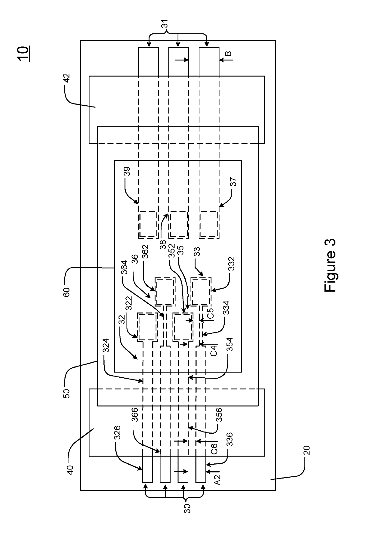
[0026]Please refer to FIG. 3, which shows a top view of the lead structure of the circuit according to the present invention applied to the chip on film package. According to the embodiment in FIG. 2, because the lead structure of the circuit according to the present invention adopts the necking design, given the same pitch, the gap in the lead structure of the circuit according to the present invention is apparently greater than the gap in the lead structure of the circuit according to the prior art. Thereby, by shrinking the gaps, the pitch of leads can be further reduced and hence enhancing the utilization efficiency of the circuit area. According to the embodiment in FIG. 3, the pitch A2, for example, 14 μm, of the lead structure of the circuit according to the present invention located on the left side of the substrate 20 is smaller than the pitch A1 according to the embodiment in FIG. 2. On the other hand, the pitch B of the lead structure of the circuit according to the prior...

third embodiment

[0030]Please refer to FIG. 5, which shows a schematic diagram of the lead structure of the circuit according to the present invention. As shown in the figure, the width of the first bump connecting part 332 is equal to the width of the second lead segment 336; the width of the second bump connecting part 352 is equal to the width of the second lead segment 356. In addition, the width of the first lead segment 334 is smaller than the width of the second lead segment 336; the width of the first lead segment 354 is smaller than the width of the second lead segment 356. Thereby, according to the embodiments in FIGS. 4 and 5, the width of the second lead segment 336 of the first lead 33 can be greater than the width of the first lead segment 334 and smaller than the width of the first bump connecting part 332.


PUM


Abstract

The present invention discloses a lead structure of the circuit, which comprises a first lead and a second lead. The first lead includes a first bump connecting part and a first lead segment. The first lead segment is connected to the first bump connecting part. The width of the first lead segment is smaller than the width of the first bump connecting part. The second lead is adjacent to the first lead and there is a lead gap therebetween. The second lead also includes a second bump connecting part and a first lead segment. The first lead segment of the second lead is connected to the second bump connecting part. The second bump connecting part and the first bump connecting part are arranged staggeredly. The second bump connecting part is adjacent to the first lead segment of the first lead.

Description

FIELD OF THE INVENTION[0001]The present invention relates generally to a lead structure of the circuit, and particularly to a lead structure of the circuit with increased gaps between adjacent leads for improving the production stability and complying with the fine pitch requirement.BACKGROUND OF THE INVENTION[0002]Owing to the increased demand in the functionality of electronic devices in recent years, the lead count of an integrated circuit (IC) in electronic devices increases accordingly, making the gaps between adjacent leads narrower. Thereby, in the packaging process for ICs, in order to fabricate more leads in a confined space for meeting the development trend of a high lead count in ICs, the lead structure in packaging needs to achieve the target of fin pitch for shrinking the gaps between adjacent leads. Unfortunately, since the gaps between adjacent leads are narrow, it is difficult for etchants to enter. Consequently, etching is difficult, or even the lead structure canno...

Claims


Application Information

Patent Timeline
IPC IPC(8): H01L23/495H01L23/00
CPCH01L23/4952H01L23/49524H01L23/49541H01L23/49582H01L24/17H01L2924/381H01L23/48H01L23/482H01L23/4985H01L2224/32225H01L2224/73204H01L2224/1416H01L2224/17154H01L2224/14154H01L23/60H01L24/13H01L24/14H01L24/16H01L24/32H01L24/73H01L24/81H01L2224/13111H01L2224/13144H01L2224/16227H01L2224/26175H01L2224/81411H01L2224/81439H01L2224/81444H01L2224/81447H01L2224/8146H01L2224/92125H01L2924/15192H01L2924/3511H01L2224/1716H01L23/49838H01L2924/00014H01L2924/01083H01L2924/013H01L2224/16225H01L2924/00
Inventor TSENG, KUO-WEICHEN, PO-CHICHENG, JUI-HSUAN
Owner SITRONIX TECH CORP
Why Eureka
Try Eureka