Substrate, method of manufacturing the same and display device

Active Publication Date: 2019-05-23
BOE TECH GRP CO LTD
View PDF10 Cites 1 Cited by
  • Summary
  • Abstract
  • Description
  • Claims
  • Application Information

AI Technical Summary

Benefits of technology

The patent describes a device with two electrodes, one of which is made of transparent conductive oxide and the other of which is made of metal. This arrangement ensures good electrical conductivity and optical clarity. The technical effect of this design is to provide a transparent electrode that combines the benefits of metal and conductive oxide, resulting in improved performance and reliability.

Problems solved by technology

In the bottom-emission OLED device, only a part of light is emitted from apertures on an array substrate and most of the light is wasted.

Method used


Image

  • Substrate, method of manufacturing the same and display device
  • Substrate, method of manufacturing the same and display device
  • Substrate, method of manufacturing the same and display device

Examples


Embodiment Construction

[0041]Embodiments of the present disclosure will be described in detail below. The embodiments described below are only used to explain the present disclosure exemplarily, and should not be construed as limiting the present disclosure. If specific techniques or conditions are not indicated in the embodiments, they are performed according to the techniques or conditions described in literatures in the related art or according to product specifications. If reagents or instruments used in the embodiments are not indicated by the manufacturers, they are all typical products that may be commercially available.

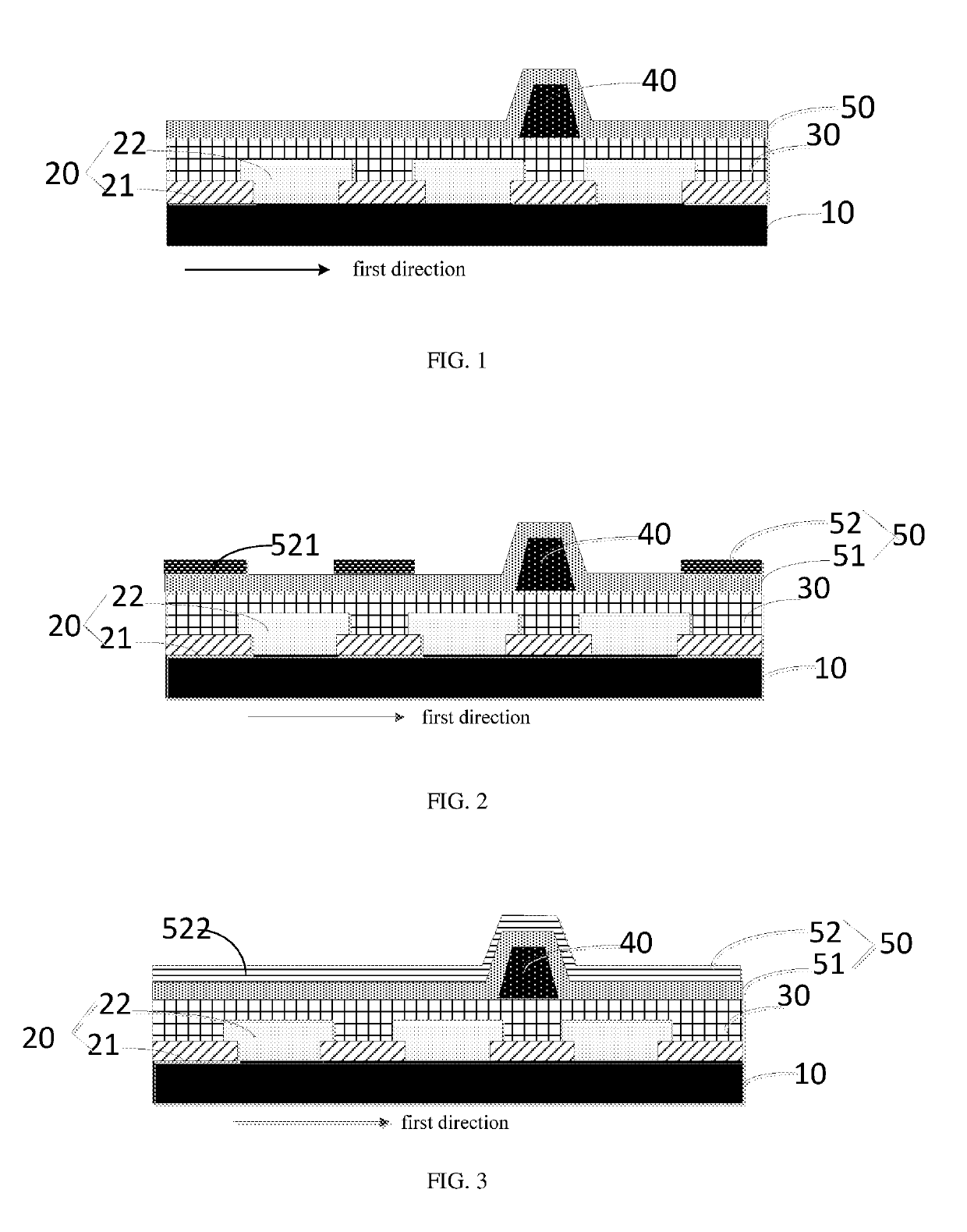
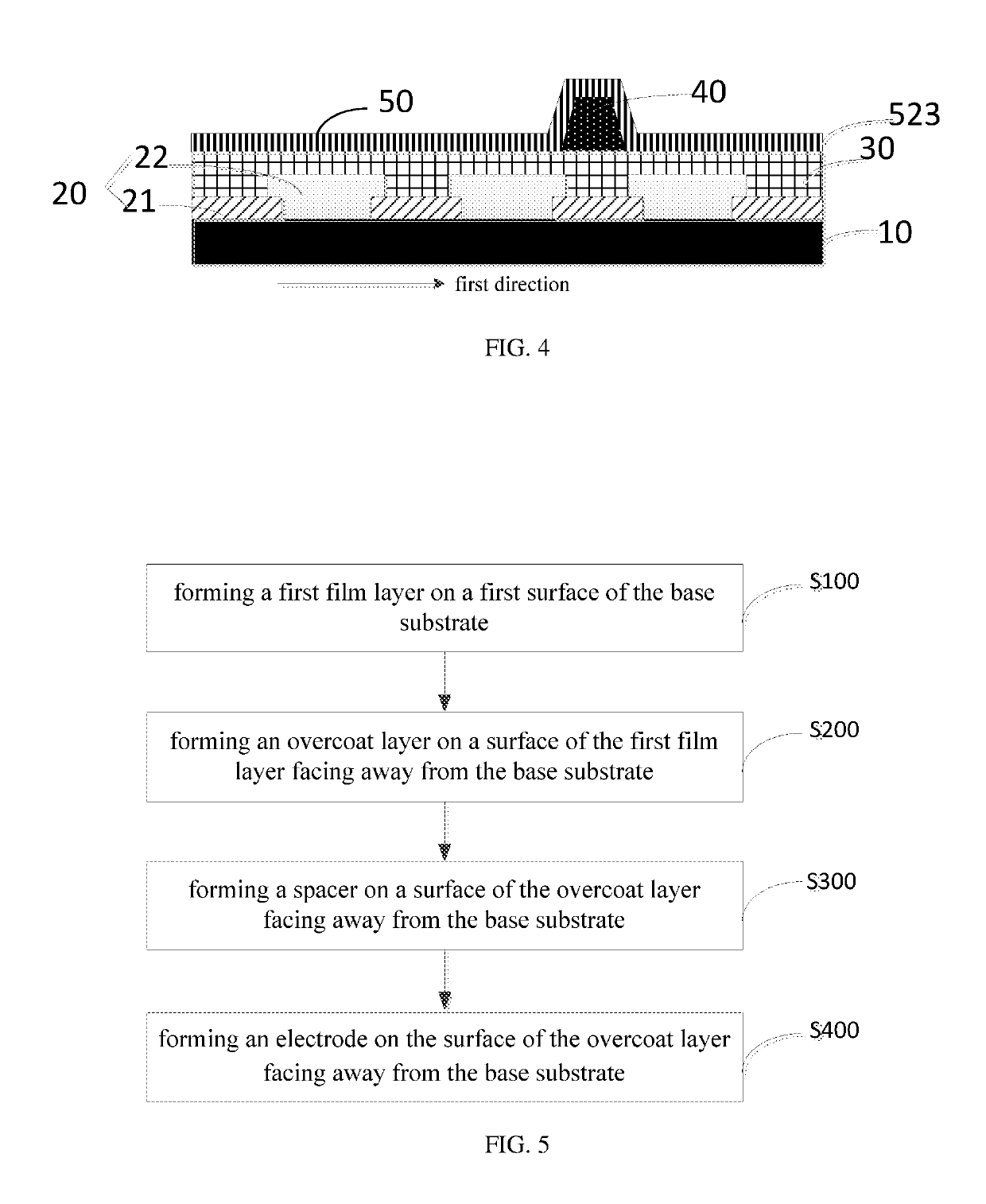
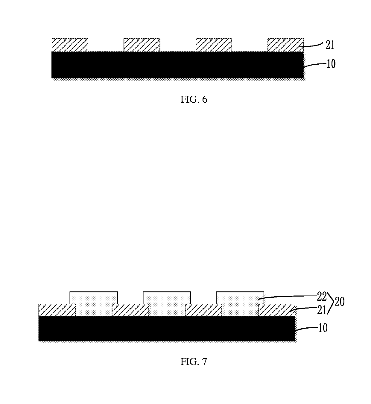
[0042]The inventors have realized that a top-emission OLED display device may be manufactured with reference to a structure of an LCD display device. For example, a top-emission structure may be achieved by a process of aligning and assembling an array substrate and a color filter substrate. Such a top-emission OLED display device typically includes a color filter substrate for the ...


PUM


Abstract

A substrate, a display device including the substrate and a method of manufacturing the substrate are disclosed. The substrate includes: a base substrate; an overcoat layer on the base substrate; and a spacer on a surface of the overcoat layer facing away from the base substrate. The spacer is in direct contact with the surface of the overcoat layer facing away from the base substrate.

Description

CROSS-REFERENCE TO RELATED APPLICATION[0001]This application claims the benefit of Chinese Patent Application No. 201711176769.9 filed on Nov. 22, 2017 in the State Intellectual Property Office of China, the whole disclosure of which is incorporated herein by reference.TECHNICAL FIELD[0002]The present disclosure relates to the field of display technology, and in particular, to a substrate, a method of manufacturing the substrate, and a display device.DESCRIPTION OF THE RELATED ART[0003]At present, OLED display devices have received more and more attention due to excellent use performances. According to different directions of light emitted from the OLED display devices, the OLED display devices may be mainly classified into two different structures: one is a bottom-emission OLED device and the other is a top-emission OLED device. In the bottom-emission OLED device, only a part of light is emitted from apertures on an array substrate and most of the light is wasted. Moreover, the bot...

Claims


Application Information

Patent Timeline
IPC IPC(8): H01L27/32H01L51/52H01L51/56
CPCH01L27/322H01L51/5234H01L27/3272H01L27/3279H01L51/56H01L51/5228H01L2251/5315H10K59/38H10K59/80516H10K59/8792H10K59/1315H10K59/8723H10K59/80517H10K2102/3026H10K50/828H10K50/865H10K50/8428H10K59/126H10K71/00H10K50/824
Inventor WANG, GUOYINGSONG, ZHEN
Owner BOE TECH GRP CO LTD
Why Eureka
Try Eureka