Scanning probe inspector
- Summary
- Abstract
- Description
- Claims
- Application Information
AI Technical Summary
Benefits of technology
Problems solved by technology
Method used
Image

Examples
Example
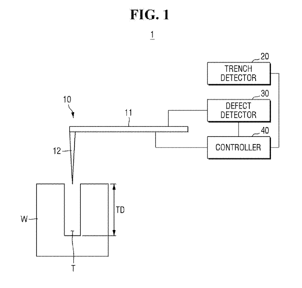
[0027]A scanning probe inspector according to some exemplary embodiments of the present disclosure can detect a defect in a trench formed in a wafer during a semiconductor manufacturing process such as fabricating a NAND flash memory or a dynamic random access memory (DRAM).
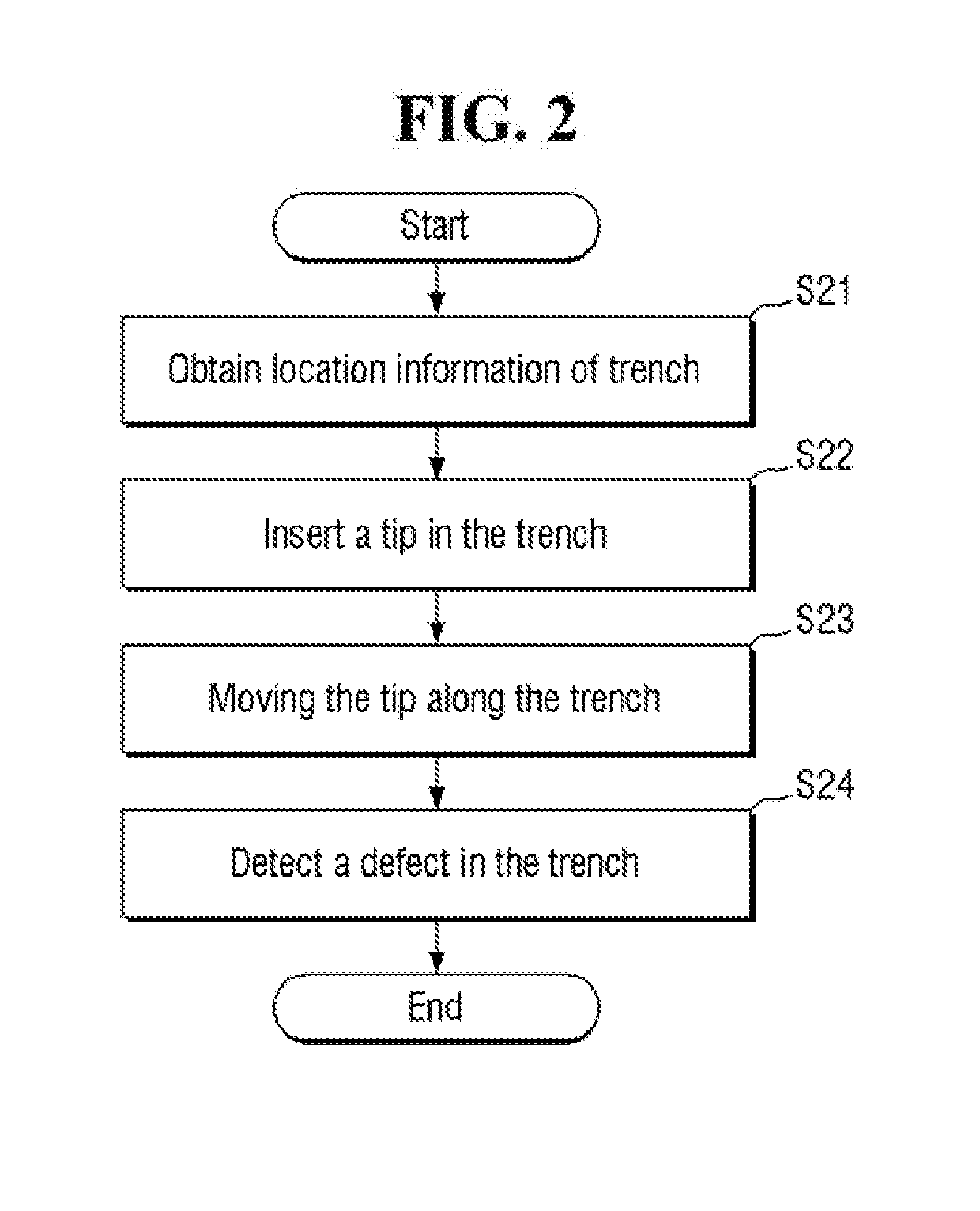
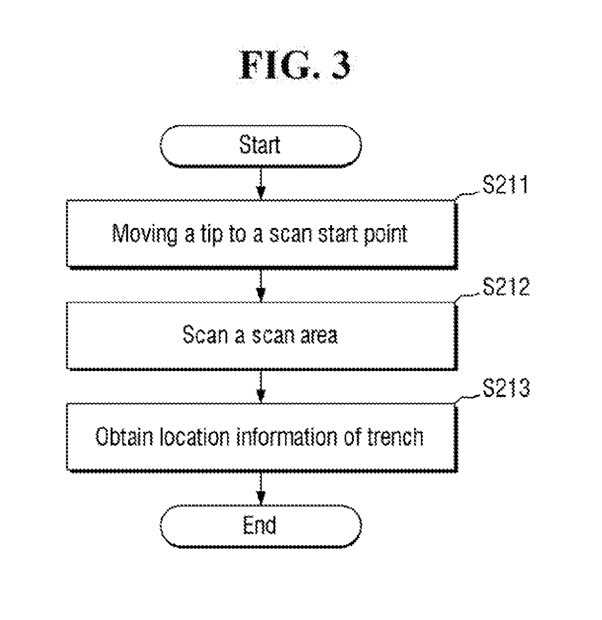
[0028]For example, the scanning probe inspector includes a tip having a length that corresponds to the height of the sidewalls of a three-dimensional (3D) structure formed in a trench during the semiconductor manufacturing process. The scanning probe inspector forms a probe junction between the tip and the sidewalls of the 3D structure by moving the tip toward the sidewalls of the 3D structure. Then, the scanning probe inspector detects a defect in the sidewalls of the 3D structure using a measurement signal generated by the probe junction. A scanning probe inspector will hereinafter be described with reference to FIGS. 1 through 23.
[0029]FIG. 1 is a schematic view of a scanning probe inspector 1 according to som...
PUM
 Abstract
Description
Claims
Application Information
 - R&D Engineer
- R&D Manager
- IP Professional
- Industry Leading Data Capabilities
- Powerful AI technology
- Patent DNA Extraction
Browse by: Latest US Patents, China's latest patents, Technical Efficacy Thesaurus, Application Domain, Technology Topic.
© 2024 PatSnap. All rights reserved.Legal|Privacy policy|Modern Slavery Act Transparency Statement|Sitemap