Near-infrared light sensors including 2-dimensional insulator

a technology of near-infrared light and insulator, which is applied in the field of near-infrared light sensors including a 2dimensional insulator, can solve the problems of eyeball damage, low sensitivity of image sensors, and needing additional light sources, and achieve the effect of improving the dark current characteristi

Active Publication Date: 2019-08-15
SAMSUNG ELECTRONICS CO LTD +1
View PDF2 Cites 8 Cited by
  • Summary
  • Abstract
  • Description
  • Claims
  • Application Information

AI Technical Summary

Benefits of technology

[0007]Some example embodiments provide one or more near-infrared light sensors having an improved dark current characteristic.

Problems solved by technology

Accordingly, when silicon-based image sensors are used for iris recognition in a low illumination environment, an additional light source is needed since the sensitivity of the image sensor is low.
However, if a high power light source is used, an eyeball may be damaged.
However, a sensor structure having favorable characteristics of photo-responsivity, dark current, and response time is limited.

Method used


Image

  • Near-infrared light sensors including 2-dimensional insulator
  • Near-infrared light sensors including 2-dimensional insulator

Examples


Embodiment Construction

[0030]Hereinafter, example embodiments of the inventive concepts will now be described in detail with reference to the accompanying drawings. In the drawings, thicknesses of layers or regions are exaggerated for clarity of specification. The embodiments of the inventive concepts are examples and capable of various modifications and may be embodied in many different forms.

[0031]It will be understood that when an element or layer is referred to as being “on” or “above” another element or layer, the element or layer may be directly on another element or layer or intervening elements or layers.

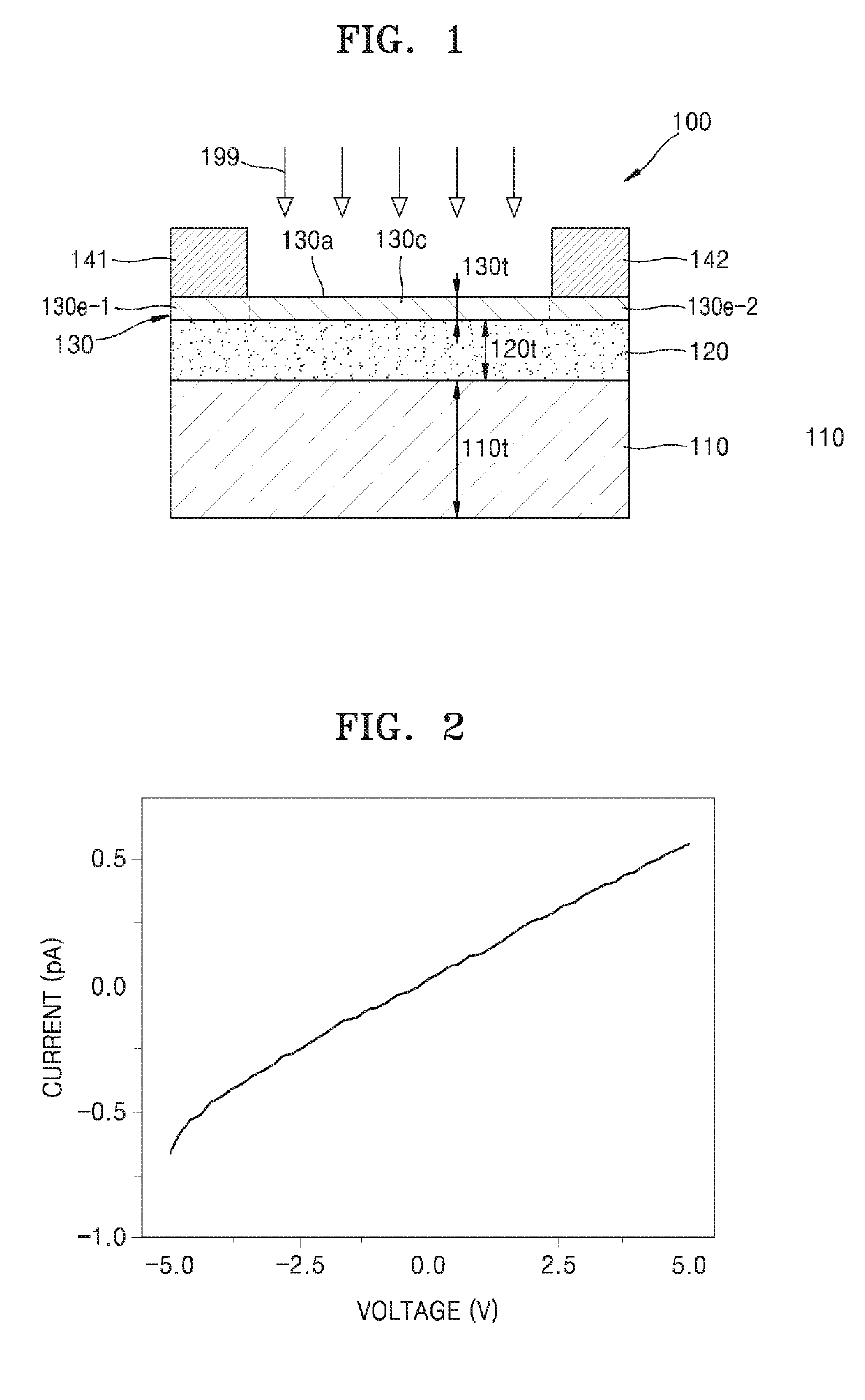
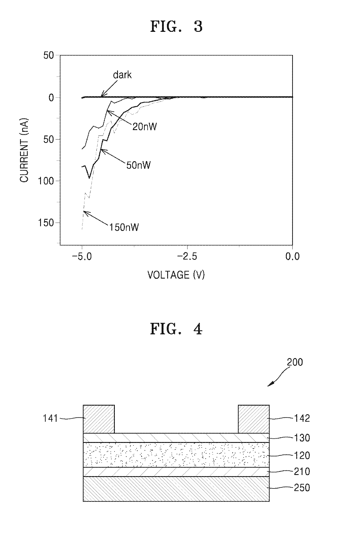
[0032]FIG. 1 is a schematic cross-sectional view of a configuration of a near infrared light sensor 100 according to some example embodiments of the inventive concepts. The near infrared light sensor 100 may include a few millions of pixels, and FIG. 1 shows one of the pixels of the near infrared light sensor 100.

[0033]Referring to FIG. 1, the near infrared light sensor 100 may include a two-dimen...


PUM


Abstract

A near infrared light sensor includes a 2D material semiconductor layer on a substrate, a tunneling layer on the 2D material semiconductor layer, and first and second electrodes on opposite edge regions of an upper surface of the tunneling layer. The 2D material semiconductor layer may be a TMDC layer having a thickness in a range of about 10 nm to about 100 nm. The tunneling layer and the substrate may each include hBN.

Description

CROSS-REFERENCE TO RELATED APPLICATION[0001]This application claims the benefit, under 35 U.S.C. § 119, of Korean Patent Application No. 10-2018-0018071, filed on Feb. 13, 2018, in the Korean Intellectual Property Office, the disclosure of which is incorporated herein in its entirety by reference.BACKGROUND1. Field[0002]The present disclosure relates to near-infrared light sensors including a 2-dimensional insulator.2. Description of the Related Art[0003]Recently, as the technique of mobile payment has been commercialized, security technology has been improved. As security technology, biometrics such as iris recognition have been studied. In the case of silicon-based image sensors that are currently commercialized, quantum efficiency with respect to a near-infrared ray (NIR) having a wavelength of 800 nm to 900 nm is approximately 30%. Since the quantum efficiency of NIR is in a level from ½ to ⅓ of a visible light band, a low illumination sensitivity of silicon-based image sensors ...

Claims


Application Information

Patent Timeline
Patent Type & Authority Applications(United States)
IPC IPC(8): H01L31/109H01L31/032H01L31/112H01L31/0224G06V40/19
CPCH01L31/109H01L31/032H01L31/0324H01L31/1129H01L31/022466H01L31/101H01L31/1136G06V40/19G06F18/00
Inventor JO, SANGHYUNYANG, HEEJUNHWANG, GEUNWOOSHIN, HYEONJIN
Owner SAMSUNG ELECTRONICS CO LTD
Why Eureka
Try Eureka