CMOS image sensor and method of operating the same

a technology of image sensor and metal oxide semiconductor, applied in the field of complementary metal oxide semiconductor (cmos) image sensor, can solve the problems of large dark current generation of 4tr structure, difficult discrimination between brightness and darkness, noise of dark current, etc., and achieve the effect of improving dark current characteristics

Active Publication Date: 2006-05-11
SAMSUNG ELECTRONICS CO LTD
View PDF15 Cites 33 Cited by
  • Summary
  • Abstract
  • Description
  • Claims
  • Application Information

AI Technical Summary

Benefits of technology

[0011] The present invention provides a complementary metal oxide semiconductor (CMOS) image sensor which has improved dark current characteristics.
[0012] The present invention also provides a method of operating a CMOS image sensor which has improved dark current characteristics.

Problems solved by technology

However, the 4Tr structure generates a relatively large dark current.
That is, the dark current is noise.
Excessively large dark current renders discrimination of brightness and darkness difficult, thereby decreasing a dynamic range.
Further, a non-uniform and excessive dark current causes a “white defect”, which generates a larger signal than normal.

Method used


Image

  • CMOS image sensor and method of operating the same
  • CMOS image sensor and method of operating the same
  • CMOS image sensor and method of operating the same

Examples


Embodiment Construction

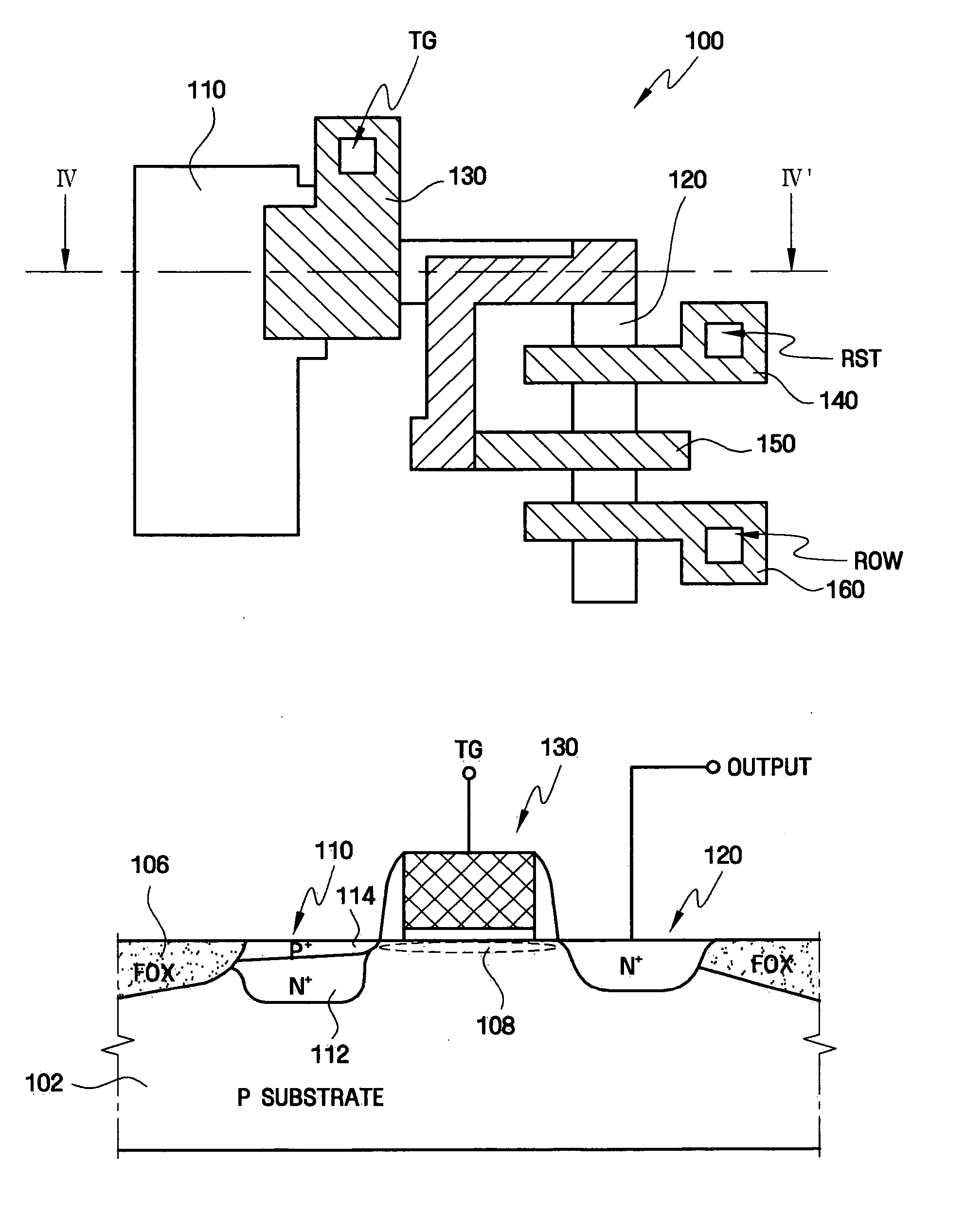
[0027] Features of the present invention and methods of accomplishing the same may be understood more readily by reference to the following detailed description of the preferred embodiments and the accompanying drawings. The present invention may, however, be embodied in many different forms and should not be construed as being limited to the embodiments set forth herein. Rather, these embodiments are provided so this disclosure will be thorough and complete and will fully convey the concept of the invention to those skilled in the art, and the present invention will be defined by the appended claims. Like reference numerals refer to like elements throughout the specification.

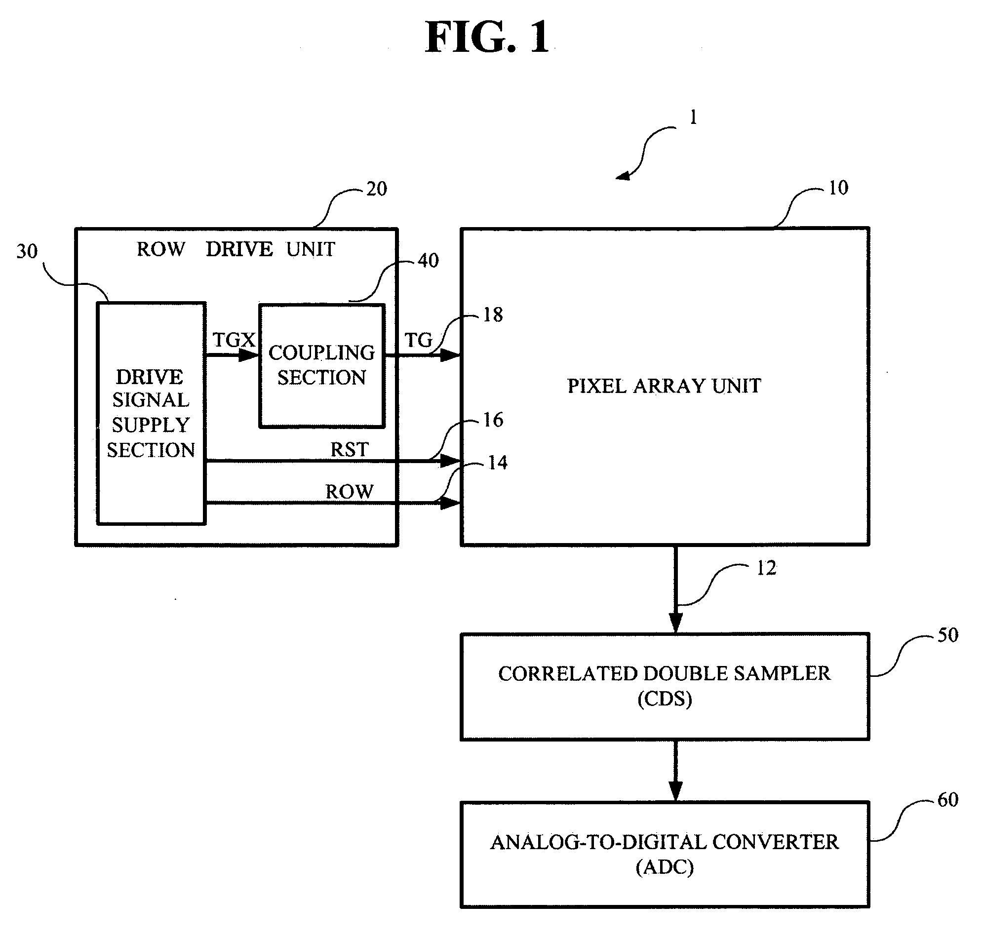
[0028]FIG. 1 is a block diagram illustrating a Complementary Metal Oxide Semiconductor (CMOS) image sensor according to an embodiment of the present invention.

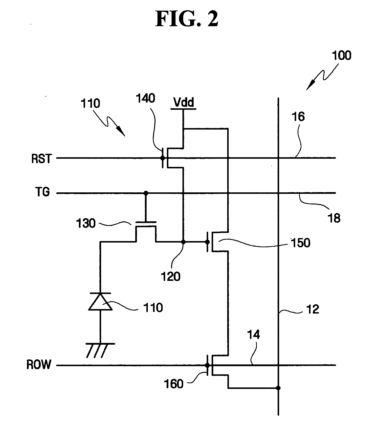
[0029] Referring to FIG. 1, a CMOS image sensor 1 includes a pixel array unit 10, a row drive unit 20, a Correlated Double Sampler (CDS) 50, and an Ana...


PUM


Abstract

A complementary metal oxide semiconductor (CMOS) image sensor and a method for operating the same are provided. The CMOS image sensor includes a pixel array unit having a matrix of pixels, wherein each pixel comprises a charge transfer element for transferring charge collected in a photoelectric conversion element to a charge detection element, and a row drive unit for supplying a voltage to the charge transfer element during part of a charge integration period of the photoelectric conversion element, wherein the supplied voltage causes the charge transfer element to have a negative potential.

Description

CROSS-REFERENCE TO RELATED APPLICATION [0001] This application claims priority from Korean Patent Application No. 10-2004-0089905 filed on Nov. 5, 2004, in the Korean Intellectual Property Office, the disclosure of which is incorporated by reference herein in its entirety. BACKGROUND OF THE INVENTION [0002] 1. Field of the Invention [0003] The present invention relates to a Complementary Metal Oxide Semiconductor (CMOS) image sensor and a method of operating the same. More particularly, the present invention relates to a CMOS image sensor with improved dark current characteristics and a method of operating the same. [0004] 2. Description of the Related Art [0005] Image sensors have been applied in various fields such as machine vision, robotics, satellite-based instrumentation, transportation, navigation, and guidance. Typically, image sensors have a two-dimensional array of pixels constituting an image frame. [0006] Pixels include photoelectric conversion elements capable of accumu...

Claims


Application Information

Patent Timeline
Patent Type & Authority Applications(United States)
IPC IPC(8): H01L31/113
CPCH01L27/14603H01L27/14609H01L27/14643H04N5/361H04N25/583H04N25/63H01L27/146H04N25/74
Inventor NAM, JUNG-HYUN
Owner SAMSUNG ELECTRONICS CO LTD
Why Eureka
Try Eureka