Embedded electronics package with multi-thickness interconnect structure and method of making same

a technology of interconnect structure and embedded chip, which is applied in the direction of logic circuit coupling/interface arrangement, logic circuit coupling arrangement, transistors, etc., can solve the problems of prior art solutions failing to provide reliable interconnect structure and complicated fabrication of embedded chip power modules having both high power semiconductor chips and low power logic semiconductor chips

Active Publication Date: 2019-10-03
GENERAL ELECTRIC CO
View PDF2 Cites 102 Cited by
  • Summary
  • Abstract
  • Description
  • Claims
  • Application Information

AI Technical Summary

Problems solved by technology

A challenge to existing manufacturing techniques is the miniaturization of electronics packages that incorporate different types of individually packaged electronics components that have different current carrying and routing density requirements, such as a mixture digital logic semiconductor devices and power semiconductor devices.
The fabrication of an embedded chip power module having both high power semiconductor chips and low power logic semiconductor chips is complicated with the concurrent need for thick and thin insulating layers, different interconnect thicknesses for high power semiconductor chips and logic semiconductor chips, and large and small vias.
However, these prior art solutions fail to provide reliable interconnect structures that efficiently provide electrical connections for logic or control semiconductor devices within the power module.

Method used


Image

  • Embedded electronics package with multi-thickness interconnect structure and method of making same
  • Embedded electronics package with multi-thickness interconnect structure and method of making same
  • Embedded electronics package with multi-thickness interconnect structure and method of making same

Examples


Embodiment Construction

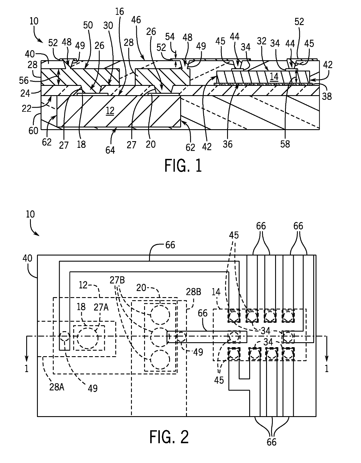
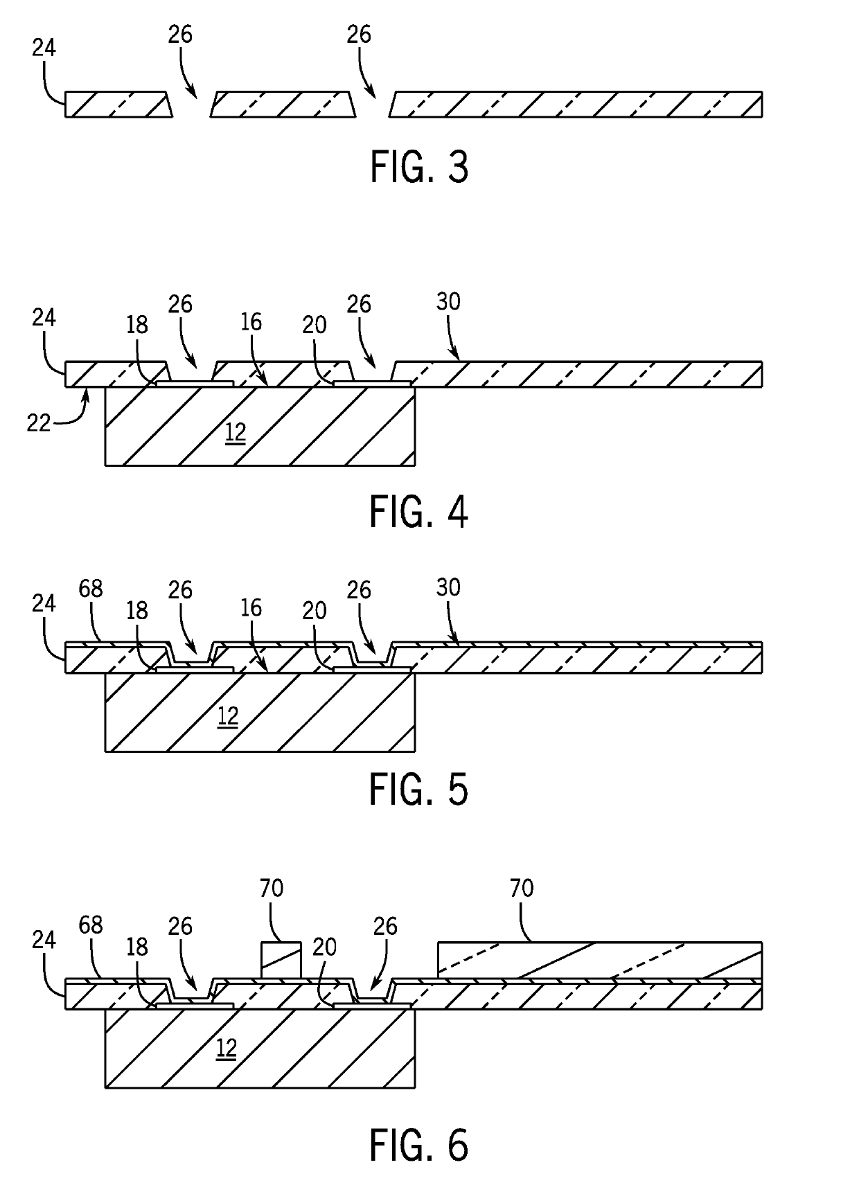
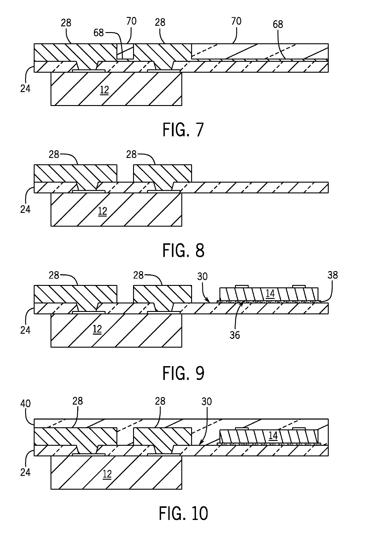
[0028]Embodiments of the present invention provide for an embedded electronics package that includes a mixture of different types of electrical components, such as a power semiconductor component and a logic semiconductor component. The electronics package includes a multi-thickness interconnect structure that includes an arrangement of thick and thin conductive interconnect layers that provide electrical interconnections for the different types of electrical components.

[0029]As used herein, the phrase “power semiconductor component” refers to a semiconductor component, device, die, or chip designed to carry a large amount of current and / or support a large voltage. As used herein, the phrase “power semiconductor device” may refer to packaged and unpackaged power semiconductor components, while the phrase “power semiconductor chip” refers to an unpackaged power semiconductor component such as diced element or die. Power semiconductor components are typically used as electrically cont...


PUM


Abstract

An embedded electronics package and method of manufacture includes a support substrate, a power semiconductor component coupled to a first side of the support substrate, and a logic semiconductor component coupled to a second side of the support substrate, opposite the first side. A first insulating material surrounds the logic semiconductor component. A logic interconnect layer is electrically coupled to the logic semiconductor component by at least one conductive micro-via extending through a portion of the first insulating material. A power interconnect layer is electrically coupled to the power semiconductor component by at least one conductive macro-via extending through a thickness of the support substrate. The power interconnect layer is thicker than the logic interconnect layer.

Description

BACKGROUND OF THE INVENTION[0001]Embodiments of the invention relate generally to structures and methods for packaging semiconductor devices and, more particularly, to an electronics package structure that facilitates the integration of different types of electrical components, such as power semiconductor devices and control or digital logic semiconductor devices, in a common package structure.[0002]As semiconductor device packages have become increasingly smaller and yield better operating performance, packaging technology has correspondingly evolved from leaded packaging, to laminated-based ball grid array (BGA) packaging, to chip scale packaging (CSP), then flip chip packages, and now buried die / embedded chip build-up packaging. Advancements in semiconductor chip packaging technology are driven by ever-increasing needs for achieving better performance, greater miniaturization, and higher reliability.[0003]A challenge to existing manufacturing techniques is the miniaturization of ...

Claims


Application Information

Patent Timeline
Patent Type & Authority Applications(United States)
IPC IPC(8): H01L23/528H01L27/088H03K19/0175H01L23/498H01L21/768H01L21/48H01L23/50H01L23/58
CPCH01L21/486H01L23/49861H01L23/49827H01L23/58H01L23/5286H01L23/50H01L27/088H03K19/017545H01L21/768H01L23/5389H01L23/5384H01L2224/18H01L25/071H01L25/18H01L2224/24137H01L2224/92144H01L24/92H01L24/82H01L24/24H01L24/19H01L24/20H01L24/29H01L2224/8385H01L2224/29386H01L2224/293H01L2224/2929H01L2224/92244H01L2224/73267H01L2224/73217H01L2224/16225H01L2924/181H01L2924/19106H01L2224/13101H01L24/13H01L24/16H01L2224/32225H01L2224/04105H01L2224/32245H01L2224/06181H01L2924/0781H01L2924/07802H01L2924/00012H01L2924/014H01L2924/00014
Inventor FILLION, RAYMOND ALBERT
Owner GENERAL ELECTRIC CO
Why Eureka
Try Eureka