Active pixel sensor with sensing circuits and output circuits disposed on the same substrate

Inactive Publication Date: 2020-01-09
SILICON OPTRONICS
View PDF0 Cites 0 Cited by
  • Summary
  • Abstract
  • Description
  • Claims
  • Application Information

AI Technical Summary

Benefits of technology

The patent text describes an active pixel sensor that includes a substrate with multiple sub-arrays arranged in a sensing array. Each sub-array has multiple pixel areas on rows and columns. Each sensing circuit includes a sensing element, a transfer transistor, and a floating diffusion node. The sensing circuits are coupled to output circuits, which are also disposed on the specific pixel row. The technical effect of this invention is to provide a more compact and efficient active pixel sensor with improved sensing and signal-to-noise ratios.

Problems solved by technology

These metal wires disadvantageously affect the light transmission of the sensing panel, which causes a dispersion phenomenon.
Thus, the amount of light sensed by each pixel is reduced, which degrades the sensing accuracy of the CMOS image sensor.

Method used


Image

  • Active pixel sensor with sensing circuits and output circuits disposed on the same substrate
  • Active pixel sensor with sensing circuits and output circuits disposed on the same substrate
  • Active pixel sensor with sensing circuits and output circuits disposed on the same substrate

Examples


Embodiment Construction

[0017]The following description is of the best-contemplated mode of carrying out the invention. This description is made for the purpose of illustrating the general principles of the invention and should not be taken in a limiting sense. The scope of the invention is best determined by reference to the appended claims.

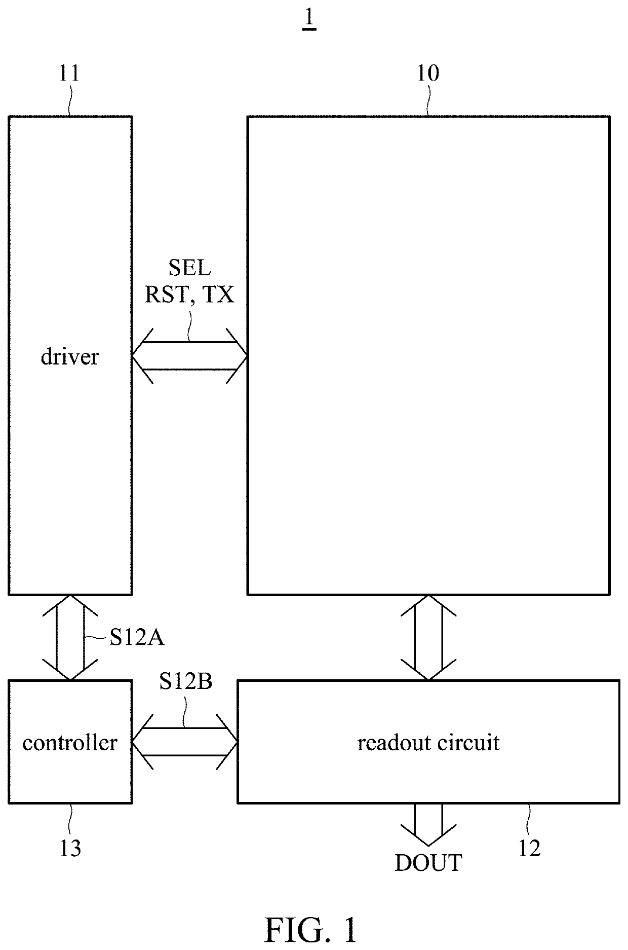
[0018]FIG. 1 shows an exemplary embodiment of an active pixel sensor. As shown in FIG. 1, an active pixel sensor 1 comprises a pixel substrate 10, a driver 11, a readout circuit 12, and a controller 13. There are a plurality of sensing circuits and a plurality of output circuits on the pixel substrate 10. The driver 11 generates various signals to control the sensing circuits and the output circuits on the pixel substrate 10 to perform an image sensing operation. The signals generated by the driver 11 comprise reset signals RST, scan signals TX, and selection signals SEL which are applied to control the sensing circuits and output circuits. The readout circuit 12 recei...


PUM


Abstract

An active pixel sensor is provided. The active pixel sensor includes a substrate comprising sub-arrays arranged to form a sensing array. For each sub-array, pixel areas are disposed on pixel rows of the sub-array. Each sub-array includes a plurality of sensing circuits and a plurality of output circuits. For each sub-array, the sensing circuits are disposed in the pixel areas on the pixel rows excluding a specific pixel row among the pixel rows. For each sub-array, the sensing circuits are further disposed on pixel columns of the sub-array to form an array, and each sensing circuit includes a sensing element, a transfer transistor, and a floating diffusion node. For each sub-array, the output circuits are disposed in the pixel areas on the specific pixel row. The sensing circuits on the same pixel column are coupled to the same output circuit.

Description

CROSS REFERENCE TO RELATED APPLICATIONS[0001]The present application is a continuation-in-part of and claims priority from U.S. patent application Ser. No. 15 / 683,082, filed Aug. 22, 2017, which claims the benefit of Taiwan application Serial No. 106121977 filed Jun. 30, 2017.BACKGROUND OF THE INVENTIONField of the Invention[0002]The invention relates to an active pixel sensor, and more particularly, to an active pixel sensor which comprises more sensing pixels and has better transmittence.Description of the Related Art[0003]Complementary metal oxide semiconductor (CMOS) image sensors have been widely used in a variety of applications, such as digital cameras and deoxyribonucleic acid (DNA) sensors, for example. Generally, each pixel on a sensing panel of a CMOS image sensor comprises a sensing element and other elements generating a corresponding sensing signal. As the size of the CMOS image sensor gets smaller, the size of the sensing element in each pixel must be reduced (that is...

Claims


Application Information

Patent Timeline
IPC IPC(8): H01L27/146H04N5/355
CPCH01L27/14643H01L27/14612H04N5/378H04N5/3559H04N25/778H04N25/76H04N25/59H04N25/75
Inventor HE, XINPING
Owner SILICON OPTRONICS
Why Eureka
Try Eureka