Semiconductor apparatus and data processing system

Active Publication Date: 2020-01-30
SK HYNIX INC
View PDF0 Cites 0 Cited by
  • Summary
  • Abstract
  • Description
  • Claims
  • Application Information

AI Technical Summary

Benefits of technology

[0009]In an embodiment, a semiconductor apparatus may include: a pad unit including a plurality of pads; a memory cell array coupled to the pad unit through input/output signal lines; and a pad configuration control circuit configured to change a pad configuration of the pad unit by dividing the plurality of pads into a plurality of groups and setting the plurality of groups to different modes, respectively.
[0010]In an embodiment, a semiconductor apparatus may include: a pad unit including a plurality of pads; write and read paths coupled to the pad unit in common through first input/ou

Problems solved by technology

Furthermore, the wide I/O semiconductor apparatus require

Method used


Image

  • Semiconductor apparatus and data processing system
  • Semiconductor apparatus and data processing system
  • Semiconductor apparatus and data processing system

Examples


Embodiment Construction

[0018]Hereinafter, a semiconductor apparatus and a data processing system according to the present disclosure will be described below with reference to the accompanying drawings through exemplary embodiments.

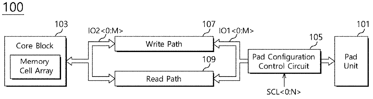
[0019]FIG. 1 illustrates a semiconductor apparatus 100 in accordance with an embodiment.

[0020]Referring to FIG. 1, the semiconductor apparatus 100 may include a pad unit 101, a core block 103, a pad configuration control circuit 105, a write path 107 and a read path 109.

[0021]The pad unit 101 may be coupled to the write path 107 and the read path 109 in common through first input and output (input / output) signal lines IO1.

[0022]The core block 103 may be coupled to the write path 107 and the read path 109 in common through second input / output signal lines IO2.

[0023]The pad unit 101 may include at least one of a plurality of pads. The plurality of pads may include data pads for inputting / outputting data, address pads for inputting addresses, command pads for inputting commands, an...


PUM


Abstract

A semiconductor apparatus may include: a pad unit including a plurality of pads; a memory cell array coupled to the pad unit through input/output signal lines; and a pad configuration control circuit configured to change a pad configuration of the pad unit by dividing the plurality of pads into a plurality of groups and setting the plurality of groups to different modes, respectively.

Description

CROSS-REFERENCES TO RELATED APPLICATION[0001]The present application claims priority under 35 U.S.C. § 119(a) to Korean application number 10-2018-0087520, filed on Jul. 27, 2018, in the Korean Intellectual Property Office, which is incorporated herein by reference in its entirety.BACKGROUND1. Technical Field[0002]Various embodiments generally relate to a semiconductor circuit, and more particularly, to a semiconductor apparatus capable of changing operation modes of signal input / output pads and a data processing system.2. Related Art[0003]A semiconductor apparatus includes a plurality of pads for outputting signals to an external device or receiving signals provided from the external device.[0004]The plurality of pads may include pads for inputting and outputting data, addresses, commands or / and separate dedicated signals.[0005]The plurality of pads may be one-to-one coupled to pins outside the semiconductor apparatus.[0006]A wide input and output (I / O) semiconductor apparatus incl...

Claims


Application Information

Patent Timeline
IPC IPC(8): G11C7/10
CPCG11C7/1048G11C7/1006G11C5/06G11C7/22G11C29/028
Inventor KIM, MYOUNG SEOLEE, SEUNG YONGJOO, YOUNG PYO
Owner SK HYNIX INC
Why Eureka
Try Eureka