Light emittng device

Active Publication Date: 2020-02-06
NICHIA CORP
View PDF4 Cites 1 Cited by
  • Summary
  • Abstract
  • Description
  • Claims
  • Application Information

AI Technical Summary

Benefits of technology

This patent describes a light emitting device that can easily connect its light emitting modules using a comb-shaped wiring board. Additionally, the device has efficient heat dissipation through heat-dissipating plates or parts arranged in the slit parts of the wiring board. These features make the device more convenient for use and improve its performance.

Problems solved by technology

However, if light emitting modules are designed to be arranged without a gap between them by bringing their side surfaces into contact with each other, it is difficult to provide space for accommodating the connecters.
For this reason, these connecters will reduce freedom of design.

Method used


Image

  • Light emittng device
  • Light emittng device
  • Light emittng device

Examples


first embodiment

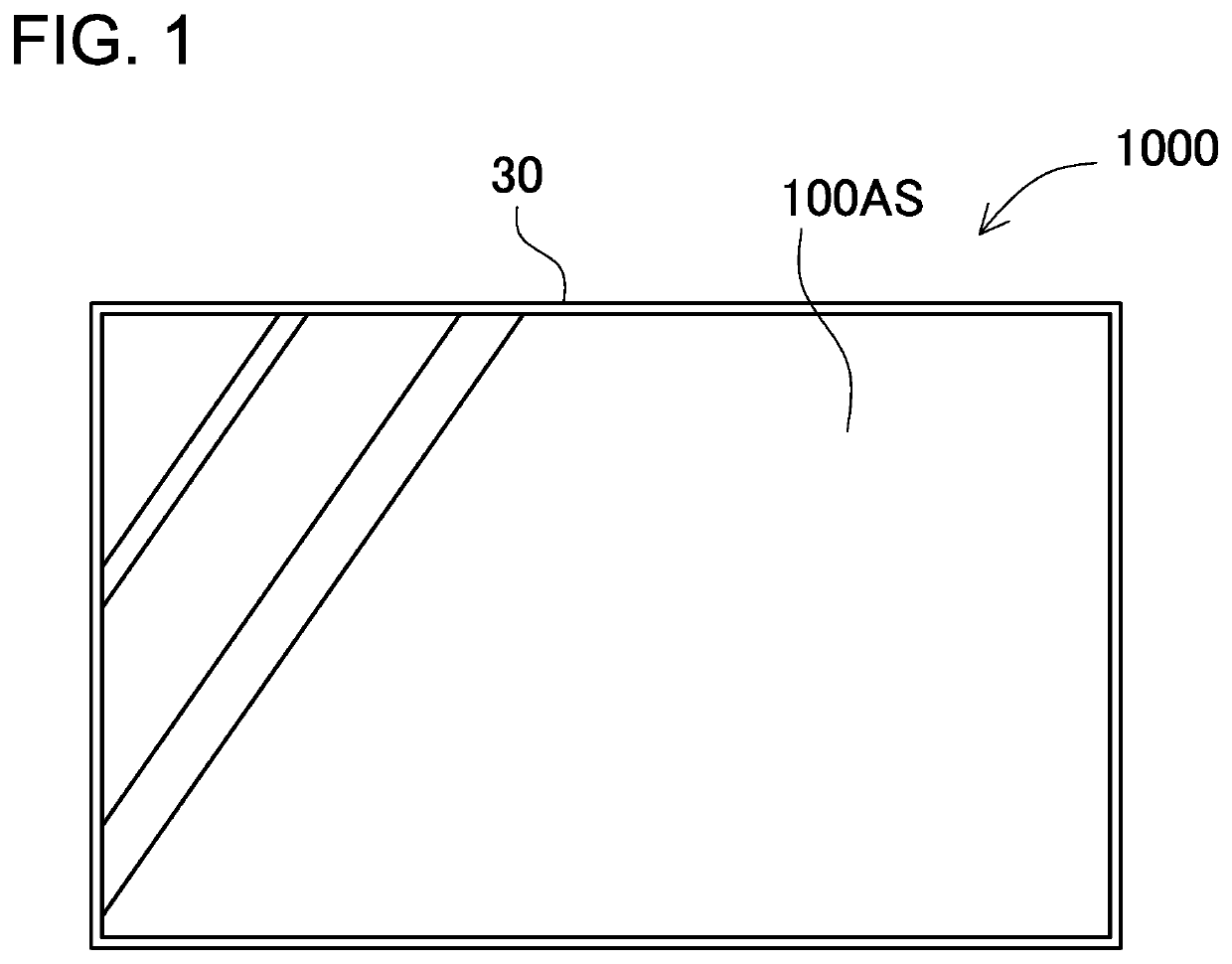
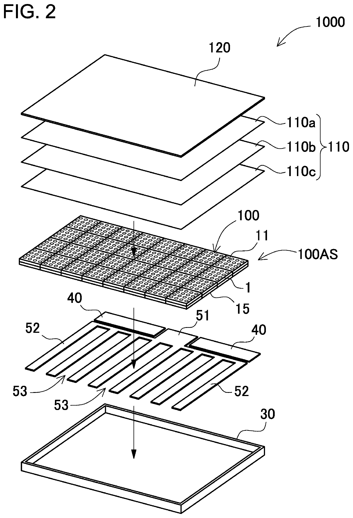
[0056]FIG. 1 is a plan view schematically showing a display 1000 which include a light emitting device according to a first embodiment. FIG. 2 shows an exploded perspective view showing the display 1000. FIG. 3 is plan view schematically showing the display 1000 without a liquid crystal panel 120 and a panel member 110 (i.e., removed from the display 1000 in FIG. 2). The illustrated display 1000 has a rectangular shape as viewed in plan view. A light emitting module assembly 100AS which includes a number of light emitting elements 11 is arranged behind the panel member 110, i.e., on the light emitting screen shown in FIG. 3. The display 1000 has a so-called direct backlight with the light emitting elements 11 being arranged on the back side of the liquid crystal panel 120. Also, the light emitting elements can be grouped into specific areas which have a certain number of light emitting elements to control ON / OFF of the specific areas of light emitting elements, i.e., to provide so-c...

modified embodiment

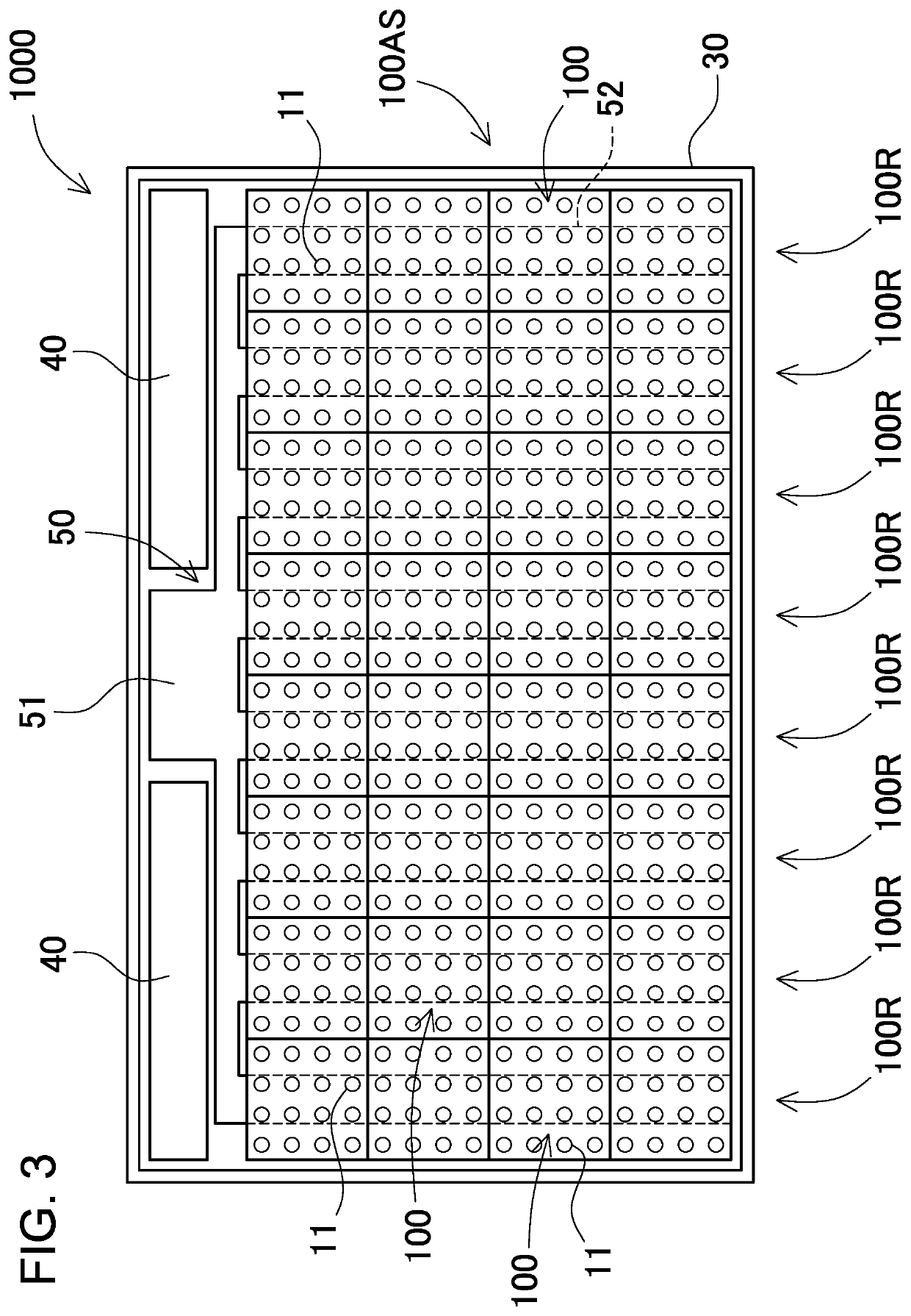
[0061]The light emitting elements 11 that is included in one light emitting module 100 are connected in series or in parallel to each other. For example, in the light emitting module 100 shown in FIG. 6, four light-emitting-element sets 11R are connected in parallel to each other. Each of the light-emitting-element sets 11R includes four light emitting elements 11, which are connected in series to each other, as shown in FIG. 6. It is noted that the connection between light emitting elements is not limited to this. For example, as shown in the light emitting device according to a modified embodiment shown in FIG. 7, eight light-emitting-element sets 11R may be connected in parallel to each other. Each of the light-emitting-element sets 11R includes two light emitting elements 11, which are connected in series to each other. This modified embodiment can be applied not only to the first embodiment but also other embodiments described later.

[0062]The light emitting module 100 includes ...

second embodiment

[0075]In the embodiment shown in FIG. 8, one comb-tooth portion 52 passes through one column of the light emitting modules 100. This arrangement can form light-emitting-module columns 100R each of which is constructed of the light emitting modules 100 that are arranged on their corresponding comb-tooth portion 52. The light emitting modules 100 in each column are connected in series to each other. In this embodiment, eight comb-tooth portions 52 are connected in parallel to each other. Specifically, eight light-emitting-module columns 100R are connected in parallel to each other. That is, one comb-tooth portion 52 passes through only one light emitting module 100 in arbitrary one row or column which is transverse to the extension line of the comb-tooth portion. However, the present invention is not limited to this arrangement. One comb-tooth portion may pass through two or more light emitting modules in arbitrary one row or column which is transverse to the extension line of the com...


PUM

PropertyMeasurementUnit
Thicknessaaaaaaaaaa
Shapeaaaaaaaaaa
Widthaaaaaaaaaa

Abstract

A light emitting device according to the present invention includes a flexible wiring board that electrically connects light emitting modules to each other. The light emitting modules include anode-side and cathode-side terminals that are arranged on their back surface and are connected to light emitting elements, which are included in their light emitting module and connected to each other in series or in parallel, in order to supply currents to light emitting elements. The wiring board has a comb shape that includes a number of comb-tooth portions extending in row or column direction of the matrix arrangement of the light emitting modules. The comb-tooth portions include an electrically-conductive pattern. The anode-side and cathode-side terminals of light emitting modules are connected to the electrically-conductive pattern of the comb-tooth portions of the wiring board.

Description

CROSS-REFERENCE TO RELATED APPLICATIONS[0001]The present application claims priority under 35 U.S.C. § 119 to Japanese Patent Application No. 2018-146,393, filed on Aug. 3, 2018, the content of which is incorporated herein by reference in its entirety.BACKGROUND OF THE INVENTION1. Field of the Invention[0002]The present invention relates to a light emitting device, a light emitting module, and a method for manufacturing the light emitting device.2. Description of the Related Art[0003]Light emitting devices that include light emitting elements such as light emitting diodes (LEDs) are widely used as backlights for liquid crystal displays, and light sources in various types of displays or the like (see Laid-Open Patent Publications Nos. JP 2012-069,673 A, and JP 2013-065,427 A, for example).[0004]In the case where such light emitting elements are used for a backlight of large liquid crystal displays, a number of light emitting elements are mounted in a matrix arrangement in a number of...

Claims


Application Information

Patent Timeline
IPC IPC(8): G02F1/1335H01L25/075H01L33/62H01L33/48H01L33/64H05K1/18
CPCG02F1/133603H01L25/0753G02F2001/133607H01L33/483G02F2001/133612G02F1/133611G02F2001/133628H05K1/189G02F1/133606H01L33/62H05K2201/10106G02F1/133608H01L33/644H01L33/642H01L27/156G02F1/133385G02F1/133612G02F1/133607H05K2201/0145H05K2201/052H05K2201/053H05K2201/10136G02F1/133628
Inventor YOSHINAGA, SATOSHISAKAMOTO, KANA
Owner NICHIA CORP
Why Eureka
Try Eureka