


Quick Research
Generate reliable direction feasibility study reports for your R&D in just a few steps.

Technical Q&A
Discover and master advanced knowledge NOW. Basics, ideas, possibilities, all at once.

Find Solutions
As an expert in R&D theories, this can generate solutions to your technical problems instantly.

Evaluate Feasibility
Analyze your overall solution with one click, know your potential R&D risks in advance.

Monitor Landscape
Get weekly tech updates, stay abreast of the latest tech innovations and key insights.
Semiconductor assembly with package on package structure and electronic device including the same
a technology of semiconductor devices and components, applied in semiconductor devices, semiconductor/solid-state device details, capacitors, etc., can solve problems such as system logical defects, and achieve the effect of reducing inductance components and minimizing existing inductance components
- Summary
- Abstract
- Description
- Claims
- Application Information
AI Technical Summary
Benefits of technology
Problems solved by technology
Method used
Image

Examples
first embodiment
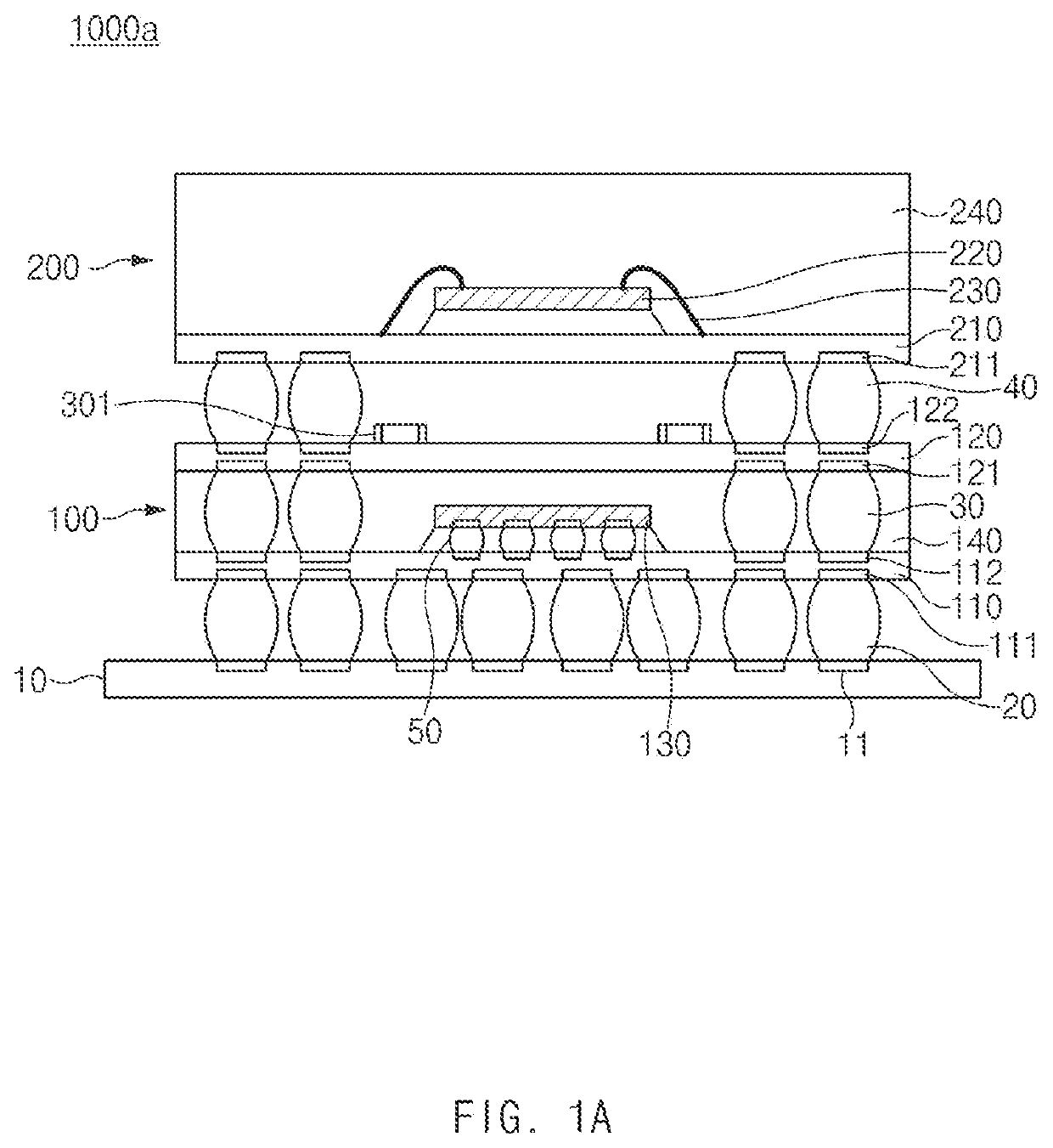
[0028]FIG. 1A is a view illustrating a form according to the present disclosure, in which a decoupling capacitor is disposed in a first semiconductor package with a POP structure.
[0029]Referring to FIG. 1A, the semiconductor assembly 1000a with a POP structure may include a first semiconductor package 100, a second semiconductor package 200, and at least one passive element 301 (e.g., a decoupling capacitor).
[0030]The semiconductor assembly 1000a with a POP structure may have a form in which a second semiconductor package 200 is stacked on the first semiconductor package 100. Then, the first semiconductor package 100 and the second semiconductor package 200 may be spaced apart from each other at a specific interval by an electrode layer (e.g., conductive bumps 40) or an insulation layer. The at least one decoupling capacitor 301 may be disposed adjacent to a semiconductor chip in the POP structure to damp a resistance or inductance component generated on a wiring path of the POP str...
second embodiment
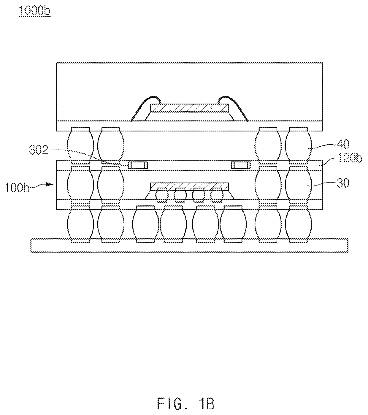
[0048]FIG. 1B is a view illustrating a form according to the present disclosure, in which a decoupling capacitor is disposed in a first semiconductor package with a POP structure.
[0049]In the second embodiment in which the decoupling capacitor 302 is disposed in the first semiconductor package 100b, the decoupling capacitor 302 may be embedded in the first upper substrate 120b. For example, the decoupling capacitor 302 may be embedded at a location of the interior area of the first upper substrate 120b, which is adjacent to the second conductive bump 30 or the third conductive bump 40. The decoupling capacitor 302 may be electrically connected to the conductive pattern included in the first upper substrate 120b. The decoupling capacitor 302 may be electrically connected to a conductive path that is the same as or corresponds to the conductive path (that is, the lower and upper conductive paths with respect to the decoupling capacitor (301 of FIG. 1A)) described with reference to FIG...
third embodiment
[0055]FIG. 2C is a view illustrating a form according to the present disclosure, in which a decoupling capacitor is disposed in a second semiconductor package with a POP structure.
[0056]In the third embodiment in which the decoupling capacitor 300c is disposed in the second semiconductor package 200c, at least a portion of the decoupling capacitor 300c may be inserted into and mounted in the second lower substrate 210c. In this regard, at least one insertion recess 212c having a specific depth may be formed on a lower surface of the second lower substrate 210c. The insertion recess 212c may have a shape and an area corresponding to those of the decoupling capacitor 300c to be firmly engaged with the decoupling capacitor 300c. Further, a fixing member or a bonding member (not illustrated) for fixing the inserted decoupling capacitor 300c may be disposed inside the insertion recess 212c. The decoupling capacitor 300c may be inserted into and mounted in the insertion recess 212c to be ...
PUM
 Abstract
Description
Claims
Application Information
 - R&D Engineer
- R&D Manager
- IP Professional
- Industry Leading Data Capabilities
- Powerful AI technology
- Patent DNA Extraction
Browse by: Latest US Patents, China's latest patents, Technical Efficacy Thesaurus, Application Domain, Technology Topic, Popular Technical Reports.
© 2024 PatSnap. All rights reserved.Legal|Privacy policy|Modern Slavery Act Transparency Statement|Sitemap|About US| Contact US: help@patsnap.com