Unlock instant, AI-driven research and patent intelligence for your innovation.
Electronic component device
Active Publication Date: 2020-04-09
MURATA MFG CO LTD
View PDF0 Cites 0 Cited by
Summary
Abstract
Description
Claims
Application Information
AI Technical Summary
This helps you quickly interpret patents by identifying the three key elements:
Problems solved by technology
Method used
Benefits of technology
Benefits of technology
The present invention relates to an electronic component device with improved heat dissipation capabilities. The device includes a first mount board and a second mount board with multiple electronic components disposed between them. The first and second mount boards are in direct contact with each other without a bonding layer in between. The electronic components are bonded to the mount boards using a bonding layer. The device also includes a second base body made of a high acoustic velocity support substrate and a low acoustic velocity film stacked on top of each other. The second base body can include a piezoelectric film stacked on top of a low acoustic velocity film. The device can have more paths through which heat can be dissipated compared to a comparative example.
Problems solved by technology
However, if heat can be dissipated through only the two heat dissipation paths mentioned above, heat generated in each mounted electronic component may not be dissipated sufficiently in some cases.
Method used
Image
Click on the blue label to locate the original text in one second.
Reading with bidirectional positioning of images and text.
Examples
embodiment
PREFERRED EMBODIMENT
1. BASIC STRUCTURE
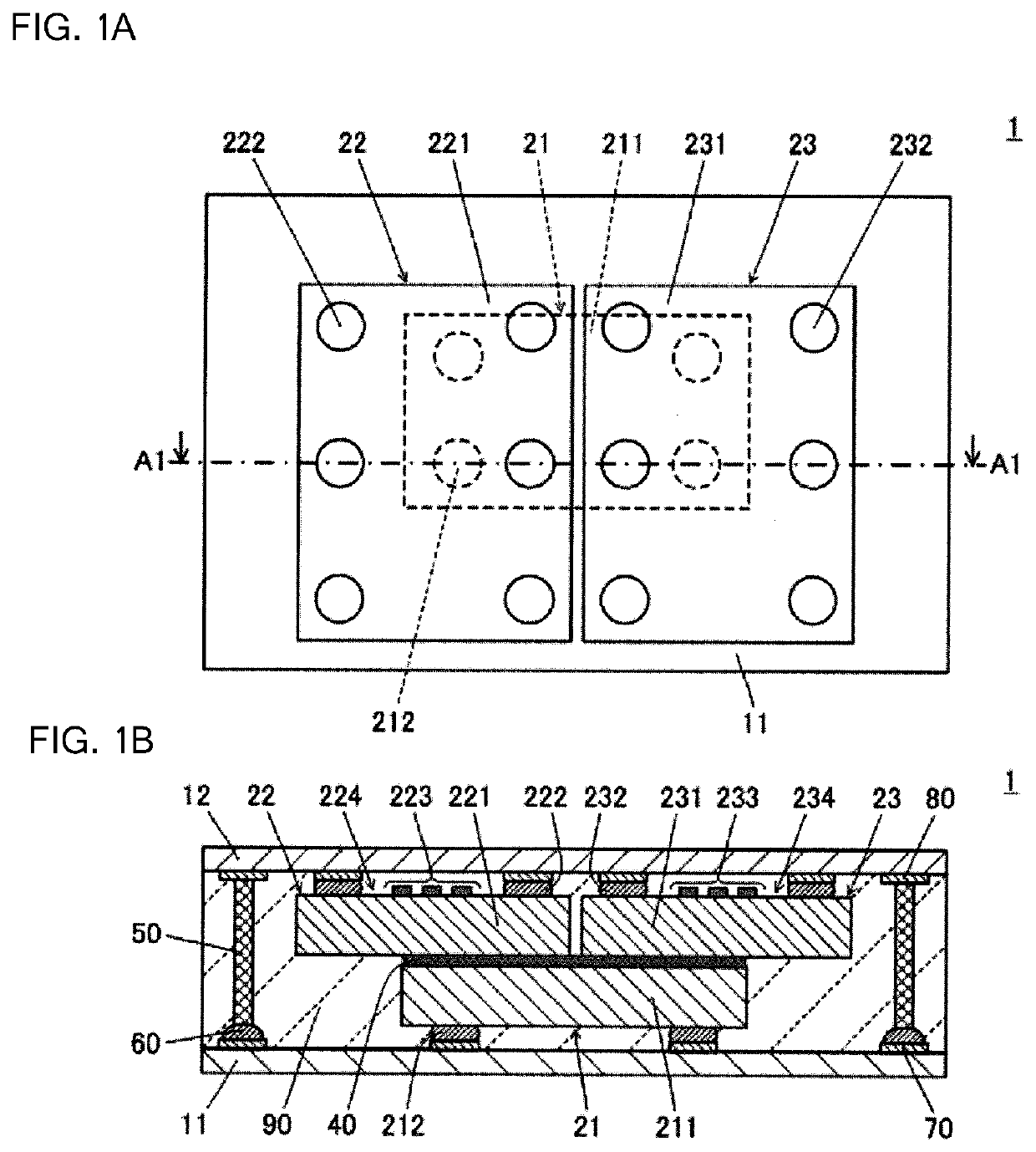
[0058]FIGS. 1A and 1B illustrate the structure of an electronic component device (module) 1 according to a preferred embodiment of the present invention. FIG. 1A is a plan view of the electronic component device 1. FIG. 1B is a cross-sectional view taken along an arrowed line A1-A1 in FIG. 1A.
[0059]In the following, for convenience of description, an electronic component 21 will be referred to as “first electronic component”, an electronic component 22 will be referred to as “second electronic component”, and an electronic component 23 will be referred to as “third electronic component”.
[0060]As illustrated in the plan view of FIG. 1A, the electronic component device 1 includes the first electronic component 21, the second electronic component 22, and the third electronic component 23. As will be described later, the first electronic component 21 includes a first base body 211, and a first outer terminal 212, which is an outer terminal of the fi...
example 1
A. Example 1
[0081]First, the following describes, as an electronic component device according to an Example 1 of a preferred embodiment of the present invention, an electronic component device in which at least two electronic components among the first electronic component 21, the second electronic component 22, and the third electronic component 23 are acoustic wave components or semiconductor components. Example 1 represents a case with a restriction placed on the type of each electronic component provided in the electronic component device 1 according to the basic structure. Accordingly, the same reference signs as those used for the electronic component device 1 according to the basic structure will be used in the following description.
I. First Aspect
[0082]In an electronic component device according to a first aspect of the Example 1, the first electronic component 21 is a semiconductor component, and the second electronic component 22 and the third electronic component 23 are a...
example 2
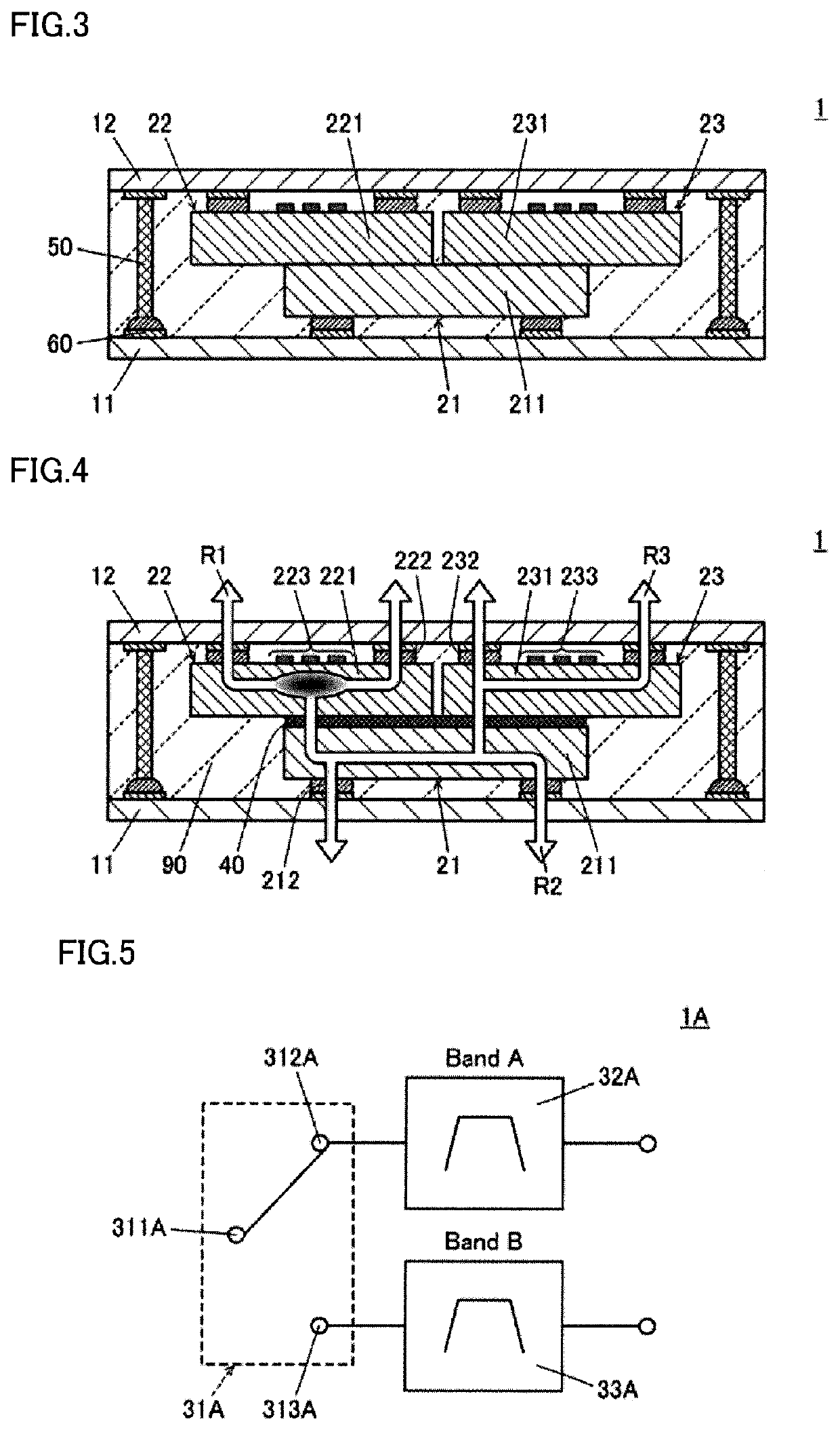
B. Example 2
[0093]The following describes, with reference to FIGS. 5 to 10, an electronic component device according to an Example 2 in which the first electronic component 21 is a switching component and the second electronic component 22 and the third electronic component 23 are filter components. The aspects of Example 2 described below each represent an example in which the electronic component device 1 according to the basic structure is an electronic component device 1A, 1B, 1C, or 1D including a switching function and a filter function.
I. First Aspect
[0094]First, an electronic component device 1A according to a first aspect of the Example 2 will be described with reference to FIGS. 5 and 6. The electronic component device 1A according to the first aspect has a switching function to perform switching for two filter components among three electronic components that define an aggregate.
[0095]FIG. 5 is a circuit diagram illustrating a circuit provided in the electronic component ...
PUM
Abstract
An electronic component device includes first and second mount boards, and first, second, and third electronic components. The first electronic component includes a first major surface and a second major surface, and is disposed on the first mount board. The first major surface is positioned closer to the first mount board than the second major surface. The second electronic component includes a third major surface and a fourth major surface, and is disposed on the second mount board. The third major surface is positioned closer to the second mount board than the fourth major surface. The third electronic component includes a fifth major surface and a sixth major surface, and is disposed on the second mount board. The fifth major surface is positioned closer to the second mount board than the sixth major surface. The second major surface directly contacts the fourth and sixth major surfaces, or indirectly contacts the fourth and sixth major surfaces with a bonding layer interposed therebetween.
Description
CROSS REFERENCE TO RELATED APPLICATIONS[0001]This application claims the benefit of priority to Japanese Patent Application No. 2017-123074 filed on Jun. 23, 2017 and is a Continuation Application of PCT Application No. PCT / JP2018 / 020102 filed on May 25, 2018. The entire contents of each application are hereby incorporated herein by reference.BACKGROUND OF THE INVENTION1. Field of the Invention[0002]The present invention relates to an electronic component device including a mount board on which plural electronic components are mounted.2. Description of the Related Art[0003]Some currently known electronic component devices have three or more electronic components mounted between two mount boards positioned to face each other. One example of such an electronic component device is a composite component disclosed in International Publication No. 2016 / 039231. The composite component has two mount boards including a first board and a second board, which is spaced apart from the first boar...
Claims
Application Information
Patent Timeline
Application Date:The date an application was filed.
Publication Date:The date a patent or application was officially published.
First Publication Date:The earliest publication date of a patent with the same application number.
Issue Date:Publication date of the patent grant document.
PCT Entry Date:The Entry date of PCT National Phase.
Estimated Expiry Date:The statutory expiry date of a patent right according to the Patent Law, and it is the longest term of protection that the patent right can achieve without the termination of the patent right due to other reasons(Term extension factor has been taken into account ).
Invalid Date:Actual expiry date is based on effective date or publication date of legal transaction data of invalid patent.

