System and method for die attach using a backside heat spreader

Active Publication Date: 2006-11-23
TEXAS INSTR INC
View PDF5 Cites 13 Cited by
  • Summary
  • Abstract
  • Description
  • Claims
  • Application Information

AI Technical Summary

Benefits of technology

[0004] Some embodiments of the invention provide numerous technical advantages. Other embodiments may realize some, none, or all of these advantages. For example, a heat conductive backside metal layer facilitates improved heat

Problems solved by technology

Decreasing power transistor sizes, among other factors, are increasing power dissipation needs.
Current die attach materials, such as solder and epoxy, may have voids therein that impact this thermal heat transfer from the chip

Method used


Image

  • System and method for die attach using a backside heat spreader
  • System and method for die attach using a backside heat spreader
  • System and method for die attach using a backside heat spreader

Examples


Example

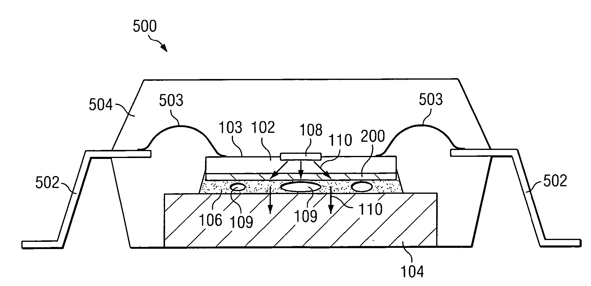
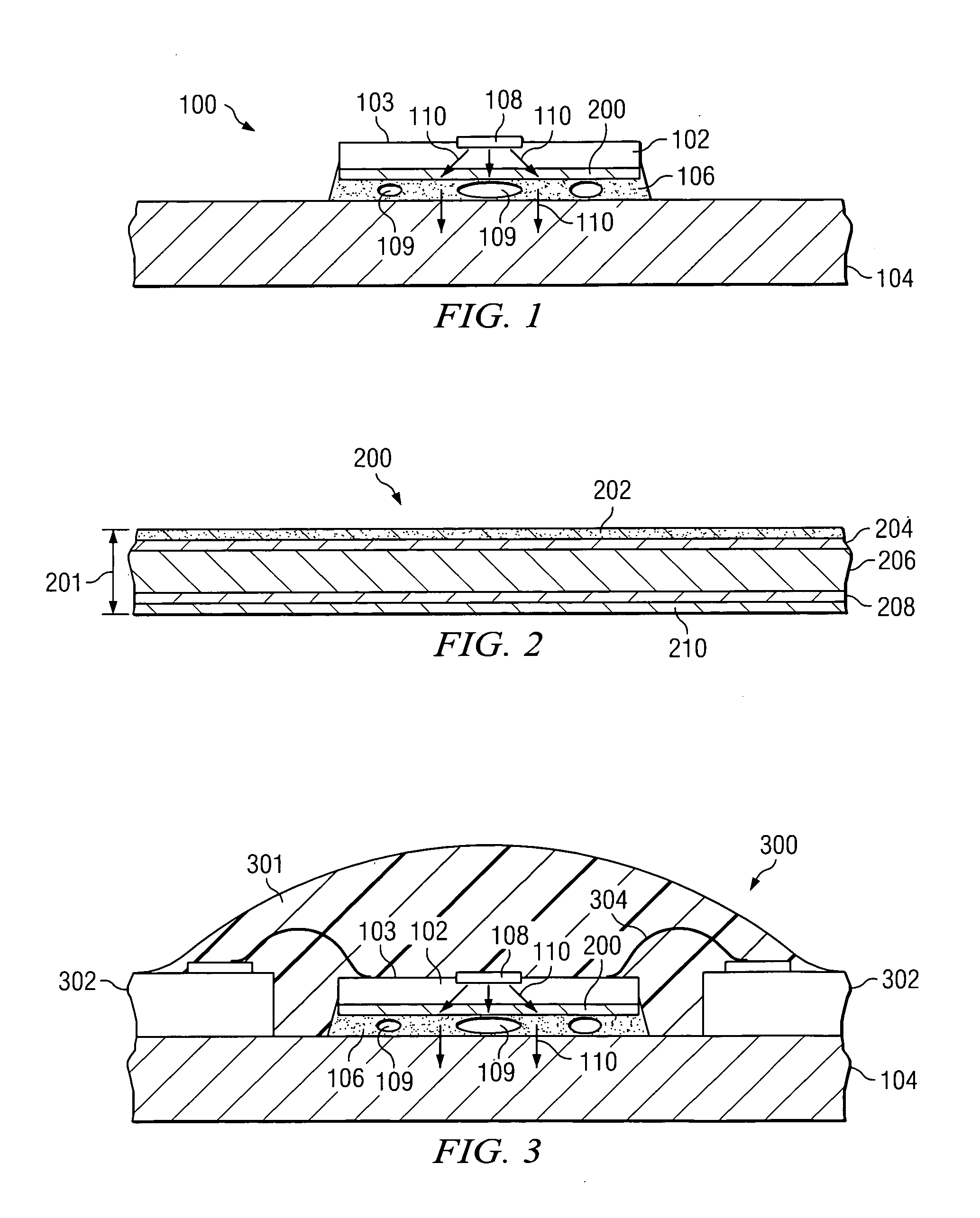
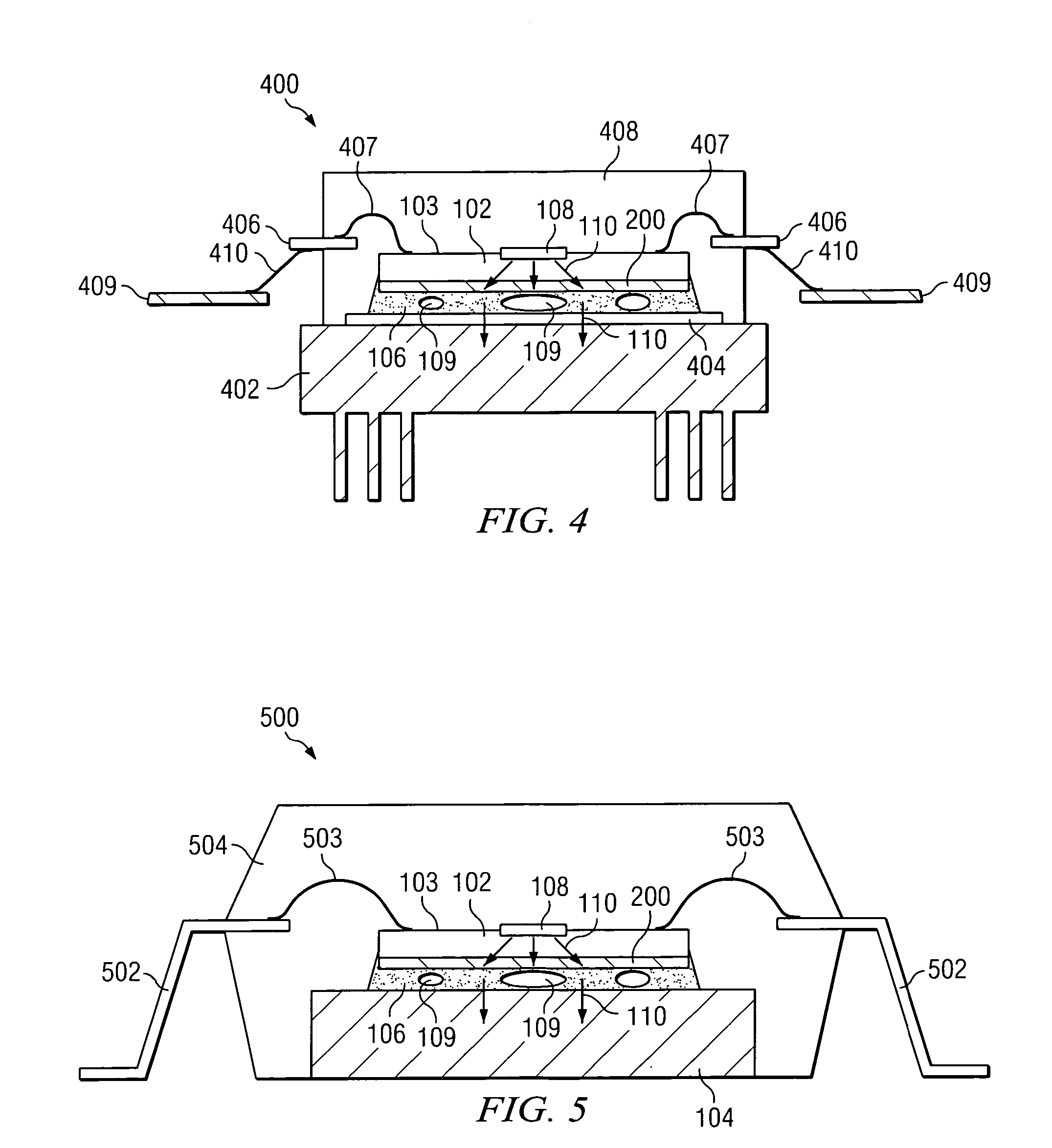
[0010] Example embodiments of the present invention and their advantages are best understood by referring now to FIGS. 1 through 5 of the drawings, in which like numerals refer to like parts.

[0011]FIG. 1 is a cross-sectional view of a die attach system 100 according to one embodiment of the invention. In the illustrated embodiment, system 100 includes a semiconductor chip 102 having a heat conductive backside metal layer 200 coupled to a substrate 104 with a die attach material 106. As described in greater detail below, heat conductive backside metal layer 200 facilitates improved heat dissipation from semiconductor chip 102 down into substrate 104.

[0012] Chip 102 may be any suitable semiconductor chip or die having any suitable size and shape and may be formed from any suitable type and number of layers of material. Chip 102 also has any suitable electronic components associated therewith. For example, as illustrated in FIG. 1, one or more power transistors 108 may be coupled to ...


PUM


Abstract

According to one embodiment of the invention, a method of die attach includes providing a chip, forming a heat conductive metal layer outwardly from a backside of the chip, and coupling the chip to a substrate. The heat conductive metal layer has a thickness of at least 0.5 mils.

Description

TECHNICAL FIELD OF THE INVENTION [0001] This invention relates generally to the field of integrated circuit packaging and, more specifically, to a system and method for die attach using a backside heat spreader. BACKGROUND OF THE INVENTION [0002] Decreasing power transistor sizes, among other factors, are increasing power dissipation needs. In an integrated circuit package, heat is typically distributed from the chip surface through the chip, through the die attach material, and through the leadframe die pad and / or external heat sink. Current die attach materials, such as solder and epoxy, may have voids therein that impact this thermal heat transfer from the chip surface. This voiding may cause local hot spots on the die surface due to decreased thermal conductivity at these spots. Overheating of the output power transistor or other chip elements can be the cause of reliability failures. SUMMARY OF THE INVENTION [0003] According to one embodiment of the invention, a method of die a...

Claims


Application Information

Patent Timeline
IPC IPC(8): H01L21/00
CPCH01L23/36H01L2224/0401H01L23/49568H01L24/32H01L2224/04026H01L2224/16H01L2224/32188H01L2224/32245H01L2224/48091H01L2224/48227H01L2224/48247H01L2224/73265H01L2924/01015H01L2924/01029H01L2924/01046H01L2924/01047H01L2924/0105H01L2924/01074H01L2924/01078H01L2924/01079H01L2924/01082H01L2924/14H01L2924/15153H01L2924/15165H01L2924/1517H01L23/4334H01L2924/01033H01L2924/01024H01L2924/01006H01L24/48H01L2924/00014H01L2924/00H01L2924/181H01L2924/00012H01L2224/45099H01L2224/45015H01L2924/207
Inventor LANGE, BERNHARD
Owner TEXAS INSTR INC
Why Eureka
Try Eureka