Light-emitting diode packaging structure

A technology for light-emitting diodes and packaging structures, applied in electrical components, electrical solid-state devices, circuits, etc., can solve problems such as inability to implement mass production, perishable packaging structures, and shortening the life of LEDs, and is suitable for mass production. It is not easy to be broken and the contact area is increased.

Inactive Publication Date: 2011-12-07
ZHANJING TECH SHENZHEN +1
View PDF11 Cites 13 Cited by
  • Summary
  • Abstract
  • Description
  • Claims
  • Application Information

AI Technical Summary

Problems solved by technology

Plastic Leaded Chip Carrier (PLCC) LEDs with lead wires in the prior art have the disadvantage of not being able to withstand high temperatures because their packaging materials and plastic lenses are prone to deterioration in high temperature environments, causing failures in the packaging structure and reducing the life of the LED. defect
Another type of LED packaging structure in the prior art uses a ceramic material with high heat transfer efficiency as the substrate of the LED chip. There is a receiving groove on the substrate. The LED chip is placed in the receiving groove and pressed together with a silicone lens. On the ceramic substrate, the LED chip is packaged on the substrate, and the heat generated by the LED chip is transmitted to the outside through the ceramic substrate. However, the ceramic substrate is relatively brittle. The center is prone to cracking, which makes it impossible to implement mass production

Method used


Image

  • Light-emitting diode packaging structure
  • Light-emitting diode packaging structure
  • Light-emitting diode packaging structure

Examples


Embodiment Construction

[0042] The present invention will be further described below in conjunction with the embodiments with reference to the accompanying drawings.

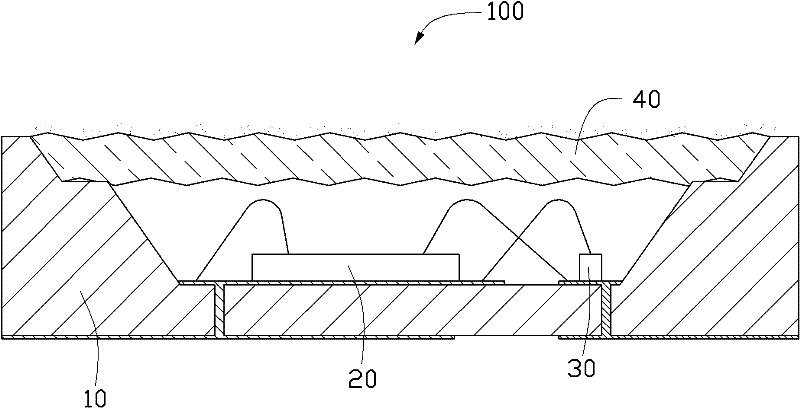
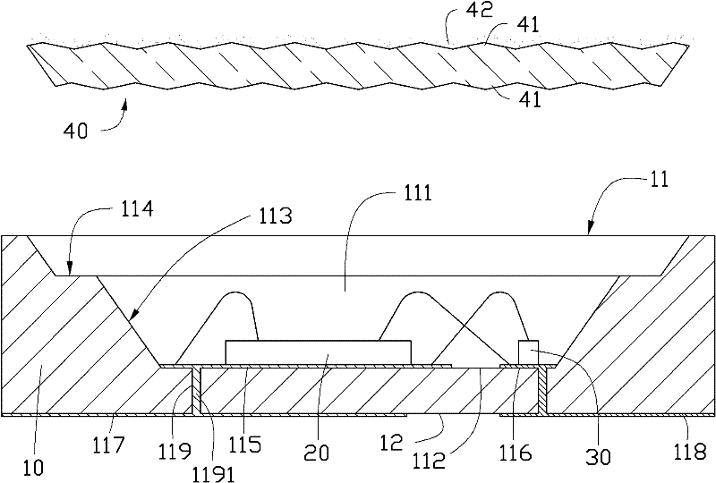
[0043] figure 1 Shown is a light emitting diode packaging structure 100 in the first embodiment of the present invention, the light emitting diode packaging structure 100 includes a substrate 10, an LED chip 20 disposed on the substrate 10, a stable structure fixed on the periphery of the LED chip 20 A voltage diode 30 and a lens 40 covering the LED chip 20 and the Zener diode 30.

[0044] Please refer to figure 2 , the substrate 10 is a silicon substrate, which can be low resistance or high resistance. To further illustrate, the high-resistance silicon substrate has a resistivity (resistivity) of about 1 to 30,000 ohm-centimeters (ohm-centimeter) and can be doped with boron (B) or phosphorus (P), while the low-resistance silicon substrate has a resistance of The ratio is about 0.001 to 0.02 ohm-cm and can be doped with boron (B), ...


PUM


Abstract

A light emitting diode package includes a silicon substrate having a first surface and a second surface opposite to the first surface, wherein the first surface includes a cavity, a light emitting diode chip fixed on a bottom of the cavity, and a glass lens secured to the silicon substrate and covering the light emitting diode chip.

Description

technical field [0001] The invention relates to a packaging structure of a photoelectric component, in particular to a packaging structure of a light emitting diode. Background technique [0002] Light emitting diodes (LEDs) in photoelectric components have the advantages of low power consumption, high brightness, small size and long service life, and are therefore considered to be the best light source for the third generation of green energy-saving lighting. [0003] With the increase of LED current intensity and light emission, the calorific value of the LED chip in the LED also increases. For high-power LEDs, 80% of the input energy is consumed in the form of heat. Plastic Leaded Chip Carrier (PLCC) LEDs with lead wires in the prior art have the disadvantage of not being able to withstand high temperatures because their packaging materials and plastic lenses are prone to deterioration in high temperature environments, causing failures in the packaging structure and reduc...

Claims


Application Information

Patent Timeline
Patent Type & Authority Applications(China)
IPC IPC(8): H01L33/48H01L33/58H01L33/62H01L33/64
CPCH01L33/486H01L2224/48091H01L2224/48227H01L33/641H01L2224/45124H01L2224/45139H01L2224/45144H01L2224/48237H01L2924/00011H01L2924/00014H01L2924/01322H01L2924/181H01L2924/00H01L2924/01004H01L2924/00012H01L2224/45015H01L2924/207
Inventor 谢明村曾文良陈隆欣林志勇
Owner ZHANJING TECH SHENZHEN
Why Eureka
Try Eureka