Touch sensor, method for manufacturing touch sensor, and image display device

a technology of touch sensor and image display device, which is applied in the direction of instruments, computing, electric digital data processing, etc., can solve the problems of impaired appearance and visible electrical pattern inside the panel, and achieve excellent covering property, suppress light reflection, and suppress light reflection

Active Publication Date: 2020-06-11
FUJIFILM CORP
View PDF0 Cites 4 Cited by
  • Summary
  • Abstract
  • Description
  • Claims
  • Application Information

AI Technical Summary

Benefits of technology

[0044]According to the embodiment of the present invention, a touch panel which suppresses the reflection of light on a bridge wire and has an excellent covering property for wiring patterns including the bridge wire is provided.
[0045]According to another embodiment of the present invention, a method for manufacturing a touch panel which suppresses the reflection of light on a bridge wire and has an excellent covering property for wiring patterns including the bridge wire is provided.
[0046]According to still another embodiment of the present invention, an image display device having improved visibility of wiring patterns including a bridge wire is provided.

Problems solved by technology

At the time of using the electrostatic capacitance-type touch panel, in a case where the surface of the touch panel is observed from, for example, a location slightly away from a location at which light incident from an internal light source is normally reflected, there is a case where the electrode patterns present inside the panel become visible and the appearance is impaired.

Method used


Image

  • Touch sensor, method for manufacturing touch sensor, and image display device
  • Touch sensor, method for manufacturing touch sensor, and image display device
  • Touch sensor, method for manufacturing touch sensor, and image display device

Examples


modification example 1

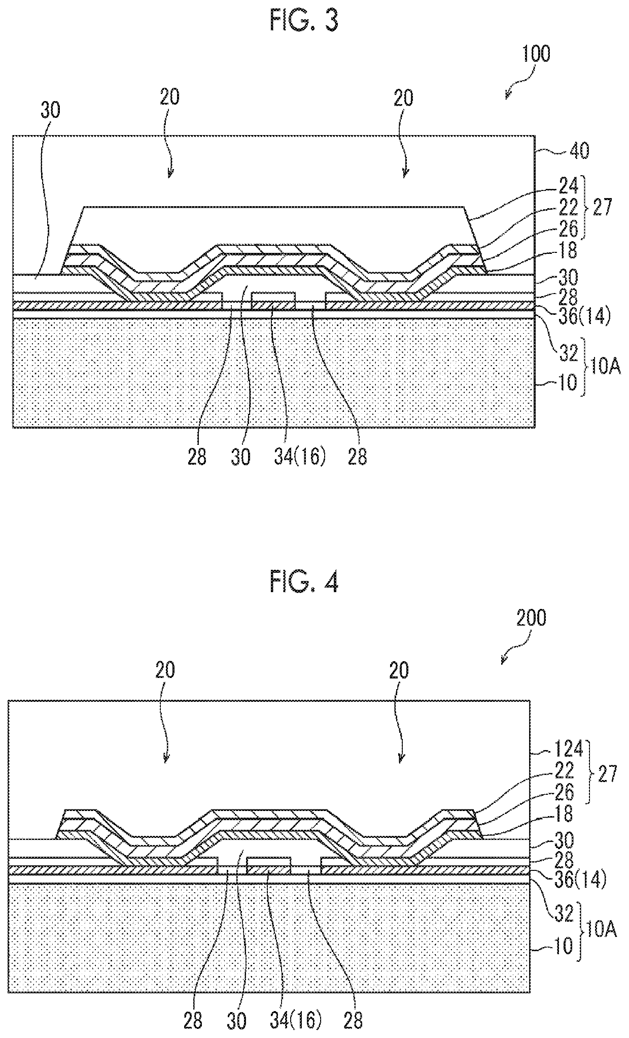
[0207]Modification Example 1 will be described with reference to FIG. 4.

[0208]A touch sensor 200 is an aspect in which, as shown in FIG. 4, instead of the fourth transparent layer 24 in FIG. 3, a fourth transparent layer 124 covering the entire surface of the electrode pattern-attached base material on which the first electrode pattern and the second electrode pattern are provided is disposed on the electrode pattern-attached base material.

[0209]In the touch sensor of the embodiment of the present disclosure, the fourth transparent layer disposed on the third transparent layer is provided to improve the visibility of the bridge wire 18, and thus, in consideration of conditions such as the shape of a product and manufacturing steps, the fourth transparent layer may be disposed to cover at least the bridge wire 18 without providing the overcoat layer 40 in FIG. 3. However, depending on cases, as shown in FIG. 3, the overcoat layer 40 is disposed as a flattening layer in order to flatt...

modification example 2

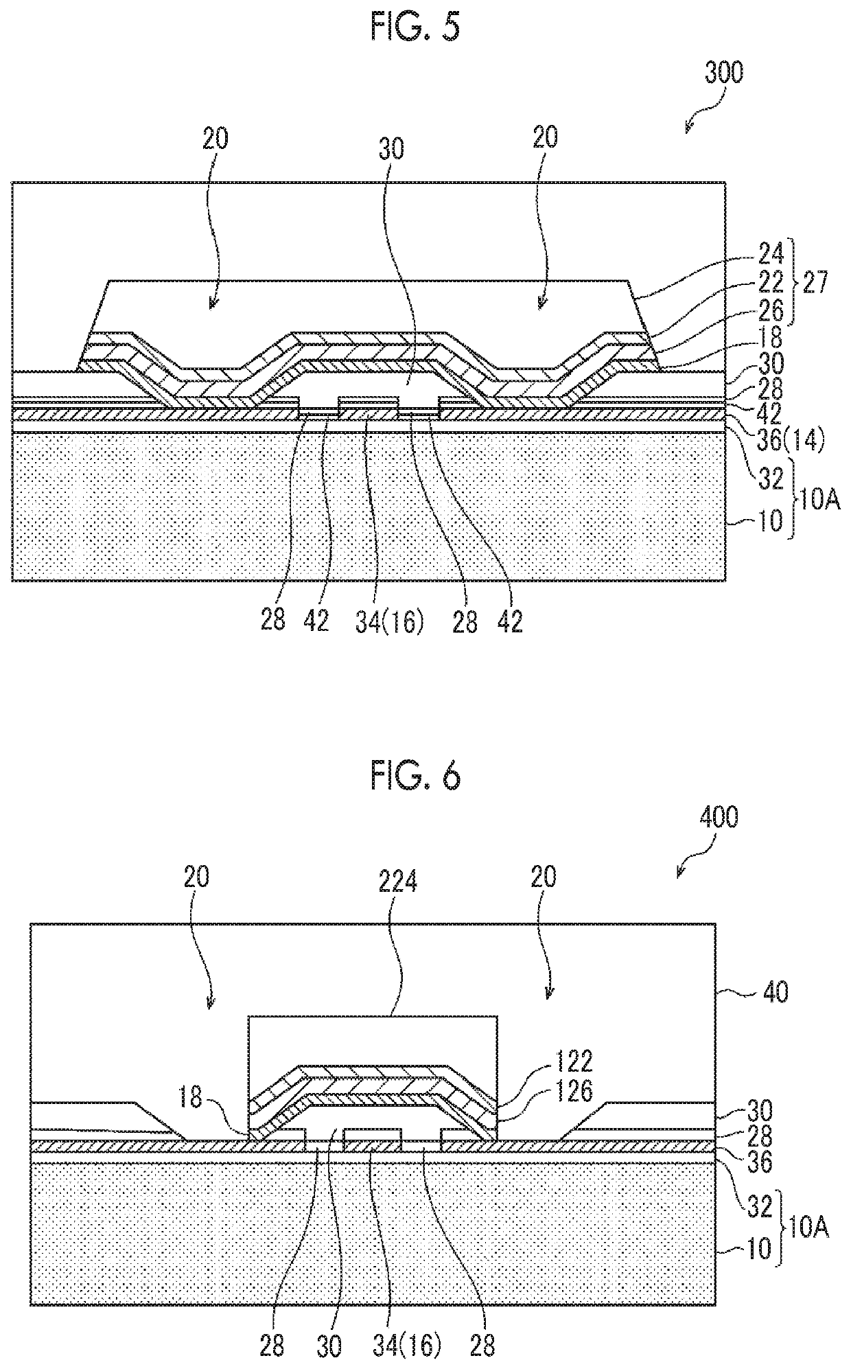
[0211]As another modification example of the touch sensor of the embodiment of the present disclosure, Modification Example 2 will be described with reference to FIG. 5.

[0212]A touch sensor 300 is an aspect in which, as shown in FIG. 5, a seventh transparent layer 42 having a refractive index of 1.5 or less and a thickness of 200 nm or less is further disposed between the first transparent layer 28 and the first electrode pattern 34 and the second electrode pattern 36.

[0213]The seventh transparent layer is preferably a low-refractive index layer having a refractive index of 1.5 or higher, and, for example, in the case of using a film having a relatively high refractive index such as an ITO film, a low-refractive index layer having a refractive index lower than that of the first transparent layer is disposed between the first transparent layer having a refractive index of 1.6 or higher and the first electrode pattern 34 and the second electrode pattern 36 in the structure. Therefore,...

modification example 3

[0214]As still another modification example of the touch sensor of the embodiment of the present disclosure, Modification Example 3 will be described with reference to FIG. 6.

[0215]A touch sensor 400 is an aspect in which, as shown in FIG. 6, the second wire portion (bridge wire) 18 building a bridge between the plurality of second island-shaped electrode portions in the second electrode pattern is in the through-hole.

[0216]In the case of such a structure, the third transparent layer and the fourth transparent layer simply need to be disposed at a location for covering at least the bridge wire 18, and thus a sixth transparent layer 126, a third transparent layer 122, and a fourth transparent layer 224 need to be disposed in accordance with the bridge wire as shown in FIG. 6.

[0217]A detection method in the touch sensor of the embodiment of the present disclosure may be any of well-known methods such as a resistance film method, an electrostatic capacitance method, an ultrasonic metho...


PUM


Abstract

A touch sensor includes a first electrode pattern and a second electrode pattern respectively extending in mutually intersecting directions on the same surface of a transparent base material, in which the second electrode pattern has a plurality of second island-shaped electrode portions disposed at intervals in a second direction intersecting the first direction and second wire portions that build bridges and electrically connect the second island-shaped electrode portions adjacent to each other on the transparent base material, and a third transparent layer having a refractive index p of 1.5 or higher and a thickness of 300 nm or less and a fourth transparent layer having a refractive index lower than the refractive index p and a thickness of 0.5 μm or more are provided in this order on the second wire portion, a method for manufacturing the same, and an image display device.

Description

CROSS-REFERENCE TO RELATED APPLICATIONS[0001]This application is a Continuation of PCT International Application No. PCT / JP2018 / 032098 filed on Aug. 30, 2018, which claims priority under 35 U.S.C § 119(a) to Japanese Patent Application No. 2017-191372 filed on Sep. 29, 2017. Each of the above application(s) is hereby expressly incorporated by reference, in its entirety, into the present application.BACKGROUND OF THE INVENTION1. Field of the Invention[0002]The present disclosure relates to a touch sensor, a method for manufacturing a touch sensor, and an image display device.2. Description of the Related Art[0003]In recent years, input devices in which information corresponding to command images can be input by touching the command images with a finger, a stylus, or the like (hereinafter, also referred to as touch panels) have been broadly used. As the touch panels, there are resistance film-type devices and electrostatic capacitance-type devices. Electrostatic capacitance-type touch...

Claims


Application Information

Patent Timeline
Patent Type & Authority Applications(United States)
IPC IPC(8): G06F3/044G06F3/041
CPCG06F3/0412G06F2203/04111G06F2203/04103G06F3/0448G06F3/0443G06F3/0446G06F3/0418
Inventor TOYOOKA, KENTAROARITOSHI, YOHEI
Owner FUJIFILM CORP
Why Eureka
Try Eureka