Display

a technology of display image and display frame, applied in the field of display image, can solve the problems of failing to achieve favorable display characteristics, and achieve the effect of excellent display image visibility

Active Publication Date: 2016-02-02
TRIVALE TECH
View PDF9 Cites 2 Cited by
  • Summary
  • Abstract
  • Description
  • Claims
  • Application Information

AI Technical Summary

Benefits of technology

[0007]It is an object of the present invention to provide a display that achieves excellent visibility of a display image even if the display is used outdoors.
[0009]The aforementioned display includes the laminated wiring and the wiring terminal part each including the translucent film and the transparent film laminated on the conductive film. This suppresses reflection of light from a surface of the conductive film, thereby obtaining a display with excellent visibility.

Problems solved by technology

Hence, if the display is used in an environment where the display receives a large amount of incident light from outside the display, the incident light reflects off a wiring made of the aluminum alloy, failing to achieve favorable display characteristics.
As described above, if the wiring is composed of a conductive film such as an aluminum alloy film, incident light reflects off a surface of the conductive film due to a high reflectance on the surface of the conductive film, failing to achieve favorable display characteristics.

Method used


Image

  • Display
  • Display
  • Display

Examples


first preferred embodiment

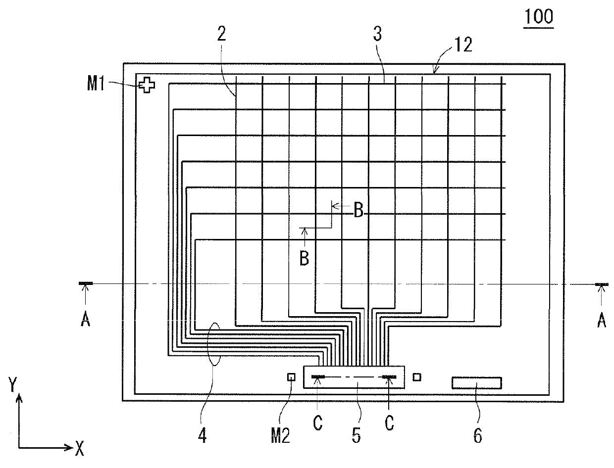
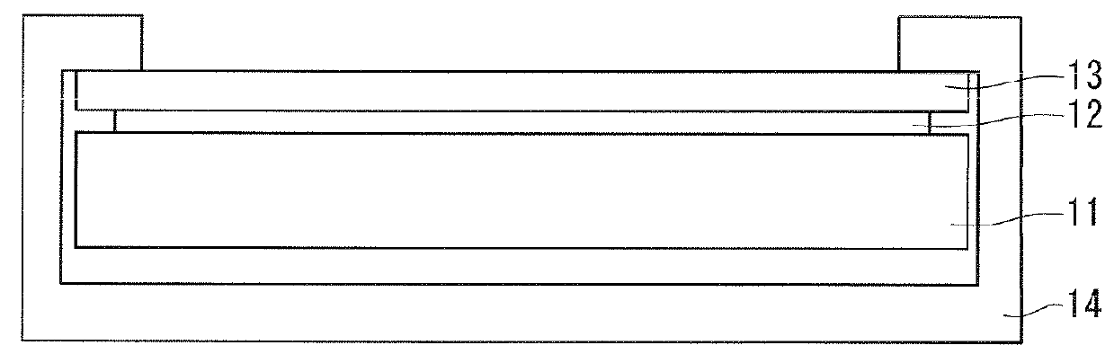
[0038]A first preferred embodiment of the present invention is described next by referring to the structure in cross section of the touch panel 12. FIG. 4 shows the structure in cross section of the touch panel 12 taken along line B-B of FIG. 1.

[0039]As shown in FIG. 4, the touch panel 12 includes a transparent substrate 20 (corresponding to a mother substrate) made for example of glass or PET, a lower wiring 30 arranged on the transparent substrate 20, and an interlayer insulating film 21 arranged so as to cover the lower wiring 30. The lower wiring 30 is a laminated wiring composed of a conductive film 31, a transparent film 32, and a translucent film 33 laminated in this order. The lower wiring 30 corresponds to the X position detecting wiring 2 shown in FIG. 1. The transparent substrate 20 functions as a foundation for forming the lower wiring 30, so that it is also called a foundation layer in some cases.

[0040]An upper wiring 40 is arranged on the interlayer insulating film 21....

second preferred embodiment

[0095]A second preferred embodiment of the present invention is described next by referring to FIGS. 24 to 28. Structures corresponding to those appearing in the manufacturing method of the first preferred embodiment described by referring to FIGS. 13 to 22 are identified by the same reference numbers, and will not be described repeatedly for the same purpose.

[0096]First, in the step shown in FIG. 24, by using an AlNiNd target, an AlNiNd film 311 to become a conductive film is deposited by sputtering process on a transparent substrate 20 to a thickness of 300 nm. Then, an ITO film 321 to become a transparent film is deposited by sputtering process on the AlNiNd film 311 to a thickness of 60 nm. Then, a Cr film 331 to become a translucent film is deposited by sputtering process on the ITO film 321 to a thickness of 5 nm. Next, an Mo film 341 to become a non low-reflection film is deposited by sputtering process on the Cr film 331 to a thickness of 10 nm.

[0097]Next, a resist material ...

third preferred embodiment

[0114]FIG. 34 shows the structure in cross section of a touch panel 12 of a third preferred embodiment. As shown in FIG. 34, the touch panel 12 of the third preferred embodiment includes: a transparent substrate 20; a lower wiring 30B, a lower wiring terminal 301B, and a mark group MK1 arranged on the transparent substrate 20; and an interlayer insulating film 21 arranged so as to cover the lower wiring 30B, the lower wiring terminal 301B, and the mark group MK1. The lower wiring 30B, the lower wiring terminal 301B, and the mark group MK1 are each a laminated wiring composed of a conductive film 31, a transparent film 32, a translucent film 33, and a transparent film 35 laminated in this order.

[0115]An upper wiring 40B and an upper wiring terminal 401B are arranged on the interlayer insulating film 21. The upper wiring 40B and the upper wiring terminal 401B are each a laminated wiring composed of a conductive film 41, a transparent film 42, a translucent film 43, and a transparent f...


PUM

PropertyMeasurementUnit
optical path lengthaaaaaaaaaa
thicknessaaaaaaaaaa
thicknessaaaaaaaaaa

Abstract

A display includes: a laminated wiring with a conductive film arranged on a foundation layer, and a transparent film and a translucent film arranged on the conductive film; a wiring terminal part arranged at an edge portion of the laminated wiring and having the same laminated structure as that of the laminated wiring; and an insulating film that covers the laminated wiring and the wiring terminal part.

Description

FIELD OF THE INVENTION[0001]The present invention relates to a display, and more specifically, to a display suitable for outdoor use.BACKGROUND ART[0002]A display to be used outdoors is required to achieve favorable display characteristics, even if it is used in an environment such as that in sunlight where the display receives a large amount of incident light from outside the display. Meanwhile, a wiring of the display is required to achieve a low resistance and required to be processed easily. An aluminum (Al) alloy responsive to these requirements has been used in many cases as a metal to form the wiring.[0003]However, an aluminum alloy has a high reflectance. Hence, if the display is used in an environment where the display receives a large amount of incident light from outside the display, the incident light reflects off a wiring made of the aluminum alloy, failing to achieve favorable display characteristics.[0004]In response, provision of an antireflection film on the aluminu...

Claims


Application Information

Patent Timeline
Patent Type & Authority Patents(United States)
IPC IPC(8): H01L33/44G02B1/116H01L51/00G02B1/11G02B1/113H05K3/06
CPCG02B1/116G02B1/113H01L33/44H05K3/061G02B1/10G02B1/11G02B5/285G06F3/041G06F2203/04103
Inventor HAYASHI, MASAMIMIYAMOTO, KENICHIISHIGA, NOBUAKITSUMURA, NAOKINAGAYAMA, KENSUKE
Owner TRIVALE TECH
Why Eureka
Try Eureka