Semiconductor devices and fabrication methods thereof

a technology of semiconductors and semiconductors, applied in semiconductor/solid-state device manufacturing, basic electric elements, electric devices, etc., can solve the problem of more serious challenges to the photolithography techniqu

Active Publication Date: 2020-09-03
SEMICON MFG INT (SHANGHAI) CORP +1
View PDF0 Cites 1 Cited by
  • Summary
  • Abstract
  • Description
  • Claims
  • Application Information

AI Technical Summary

Benefits of technology

[0024]However, in order to ensure a distance from the region where the first trench 121 is intended to be divided to the region of the separation mask layer 131 in the second direction Y, the separation structure may not extend to the first mask layer 120 corresponding to the position of the second trench 150, such that the size of the separation structure in the first direction X may have fewer restrictions. In order to ensure a small distance between the two first sub-trenches on the two sides of the separation structure, the size of the separation structure in the second direction Y needs to be small. As such, the separation structure not only needs to have a small size in the first direction, but also requires a small size in the second direction. The position of the separation structure is directly defined by the lithography opening formed in the lithography layer. Therefore, the size of the lithography opening needs to be small in both the first direction and the second direction, and thus the challenge to the photolithography process may be significant, and the process difficulty may also increase.

Problems solved by technology

With the size of semiconductor device continuously becoming smaller, the critical photolithography dimension gradually approaches or even exceeds the physical limits of the photolithography process, which leads to more serious challenges to the photolithography technique.

Method used


Image

  • Semiconductor devices and fabrication methods thereof
  • Semiconductor devices and fabrication methods thereof
  • Semiconductor devices and fabrication methods thereof

Examples


Embodiment Construction

[0013]Reference will now be made in detail to exemplary embodiments of the invention, which are illustrated in the accompanying drawings. Wherever possible, the same reference numbers will be used throughout the drawings to refer to the same or like parts.

[0014]FIGS. 1-5 illustrate schematic views of semiconductor structures at certain stages of a fabrication process of a semiconductor device.

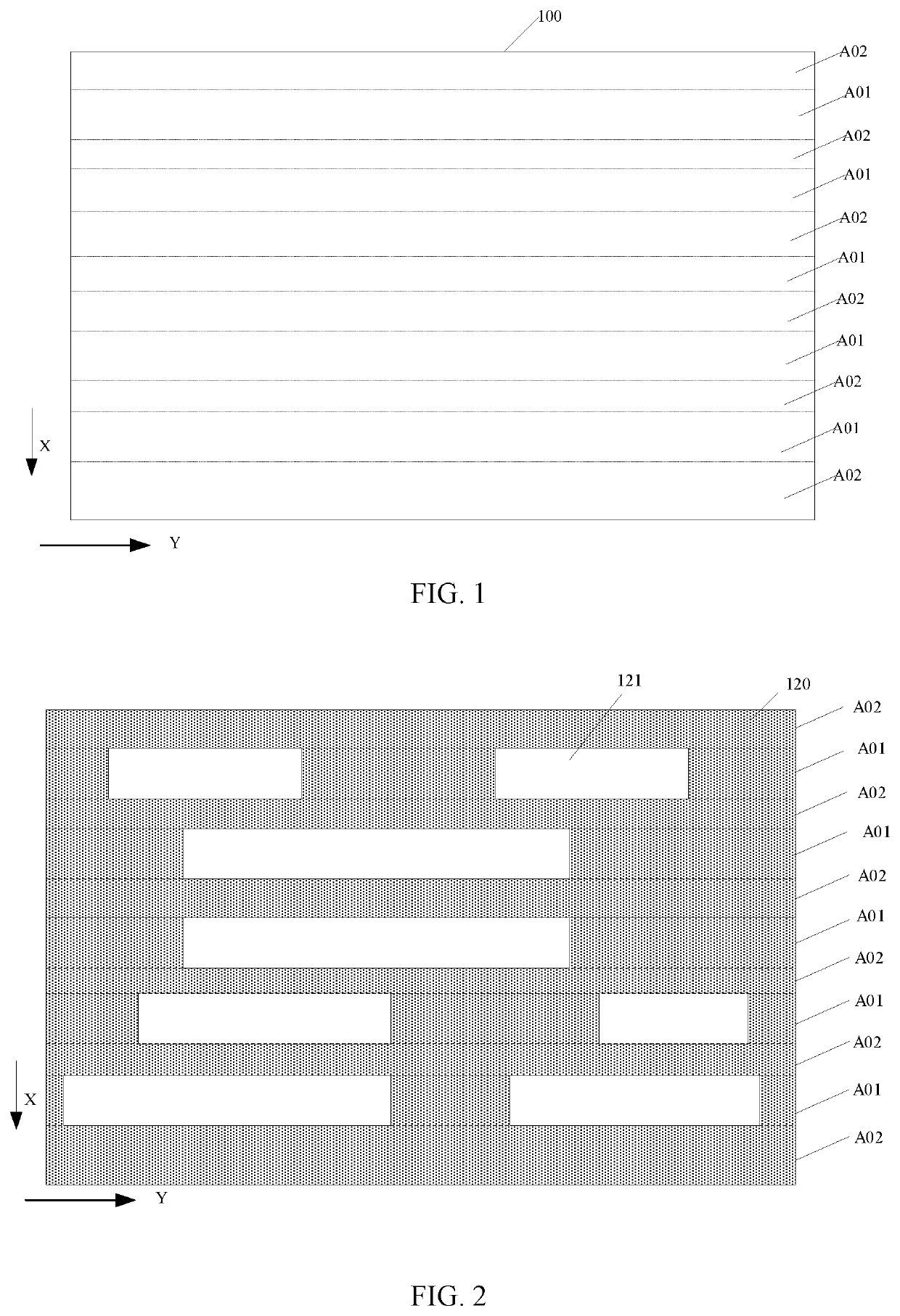
[0015]Referring to FIG. 1, a to-be-etched layer 100 is provided. The to-be-etched layer 100 includes a plurality of discrete first regions A01 and a plurality of discrete second regions A02. The plurality of first regions A01 and the plurality of second regions A02 are arranged alternately along a first direction X. For a first region A01 adjacent to a second region A02, the first region A01 and the second region A02 adjoin each other, e.g., the first region A01 and the second region A02 share an edge.

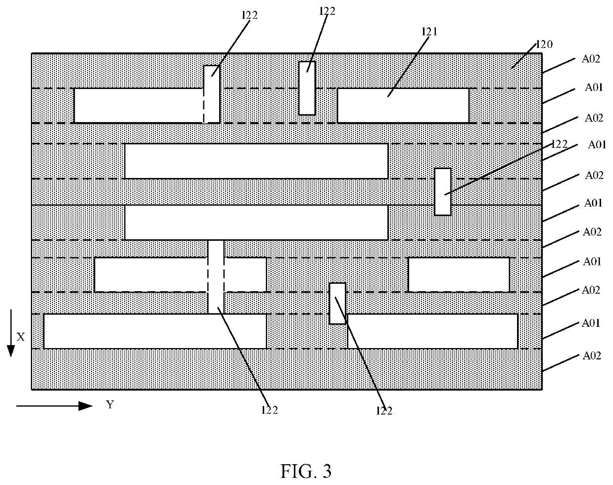
[0016]Referring to FIG. 2, a first mask layer 120 is formed on the plurality of first regions ...


PUM

PropertyMeasurementUnit
sizeaaaaaaaaaa
sizeaaaaaaaaaa
widthaaaaaaaaaa

Abstract

A method for fabricating a semiconductor device includes providing a to-be-etched layer, including alternately arranged first regions and second regions along a first direction. Each second region includes a trench region. The method includes forming a first mask layer on the to-be-etched layer; forming a doped separation layer in the first mask layer on the second region of the to-be-etched layer to divide the first mask layer along a second direction perpendicular to the first direction; forming a first trench in the first mask layer on the first region; forming a separation filling layer to divide the first trench along the second direction; implanting doping ions into the first mask layer outside of the trench region; and removing the first mask layer formed in the trench region on both sides of the doped separation layer to form a second trench that is divided into portions along the second direction.

Description

CROSS-REFERENCES TO RELATED APPLICATIONS[0001]This application claims the priority of Chinese Patent Application No. CN201910155834.2, filed on Mar. 1, 2019, the entire content of which is incorporated herein by reference.FIELD OF THE DISCLOSURE[0002]The present disclosure generally relates to the field of semiconductor fabrication technology and, more particularly, relates to semiconductor devices and fabrication methods thereof.BACKGROUND[0003]In the process of fabricating semiconductor devices, a photolithography process is usually adopted to transfer the pattern from a mask to a substrate. The photolithography process includes: providing a substrate; forming a photoresist layer on the substrate; exposing and developing the photoresist layer to form a patterned photoresist layer, such that the pattern on the mask is transferred to the photoresist layer; etching the substrate using the patterned photoresist layer as a mask, such that the pattern on the photoresist layer is transfe...

Claims


Application Information

Patent Timeline
Patent Type & Authority Applications(United States)
IPC IPC(8): H01L21/033H01L21/027
CPCH01L21/31155H01L21/0276H01L21/0337H01L21/31144H01L21/76816Y02P70/50
Inventor JIN, JISONG
Owner SEMICON MFG INT (SHANGHAI) CORP
Why Eureka
Try Eureka