Semiconductor device and fabrication method thereof

a semiconductor and semiconductor technology, applied in the field of semiconductor device, can solve the problems of substantially serious photolithography challenges and the difficulty of a conventional process for and achieve the effect of substantially high difficulty in forming the semiconductor devi

Active Publication Date: 2020-09-03
SEMICON MFG INT (SHANGHAI) CORP +1
View PDF0 Cites 1 Cited by
  • Summary
  • Abstract
  • Description
  • Claims
  • Application Information

AI Technical Summary

Problems solved by technology

As the size of the semiconductor device continues to shrink, the critical dimension in photolithography gradually approaches or even exceeds the physical limits of photolithography, which poses substantially serious challenges for photolithography.
However, the difficulty of a conventional process for forming the semiconductor device is substantially high.

Method used


Image

  • Semiconductor device and fabrication method thereof
  • Semiconductor device and fabrication method thereof
  • Semiconductor device and fabrication method thereof

Examples


Embodiment Construction

[0014]Reference will now be made in detail to exemplary embodiments of the disclosure, which are illustrated in the accompanying drawings. Wherever possible, the same reference numbers will be used throughout the drawings to refer to the same or the alike parts.

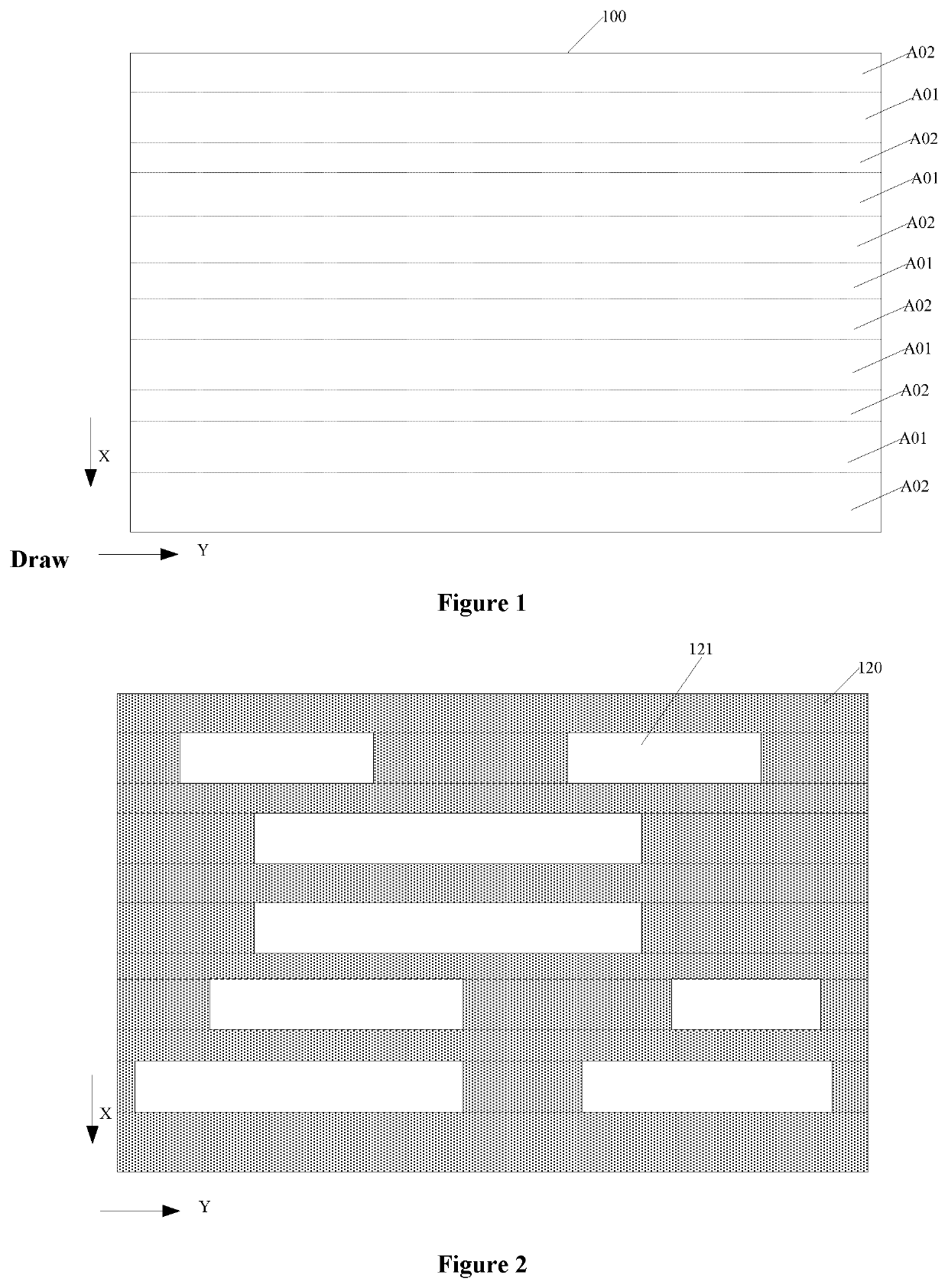
[0015]FIGS. 1-5 illustrate semiconductor structures corresponding to certain stages for forming a semiconductor device. Referring to FIG. 1, a layer 100 to-be-etched is provided. The layer 100 to-be-etched includes a plurality of first regions A01 and a plurality of second regions A02. The first regions A01 and the second regions A02 are alternately arranged along a first direction X. The first region A01 is in contact with an adjacent second region A02.

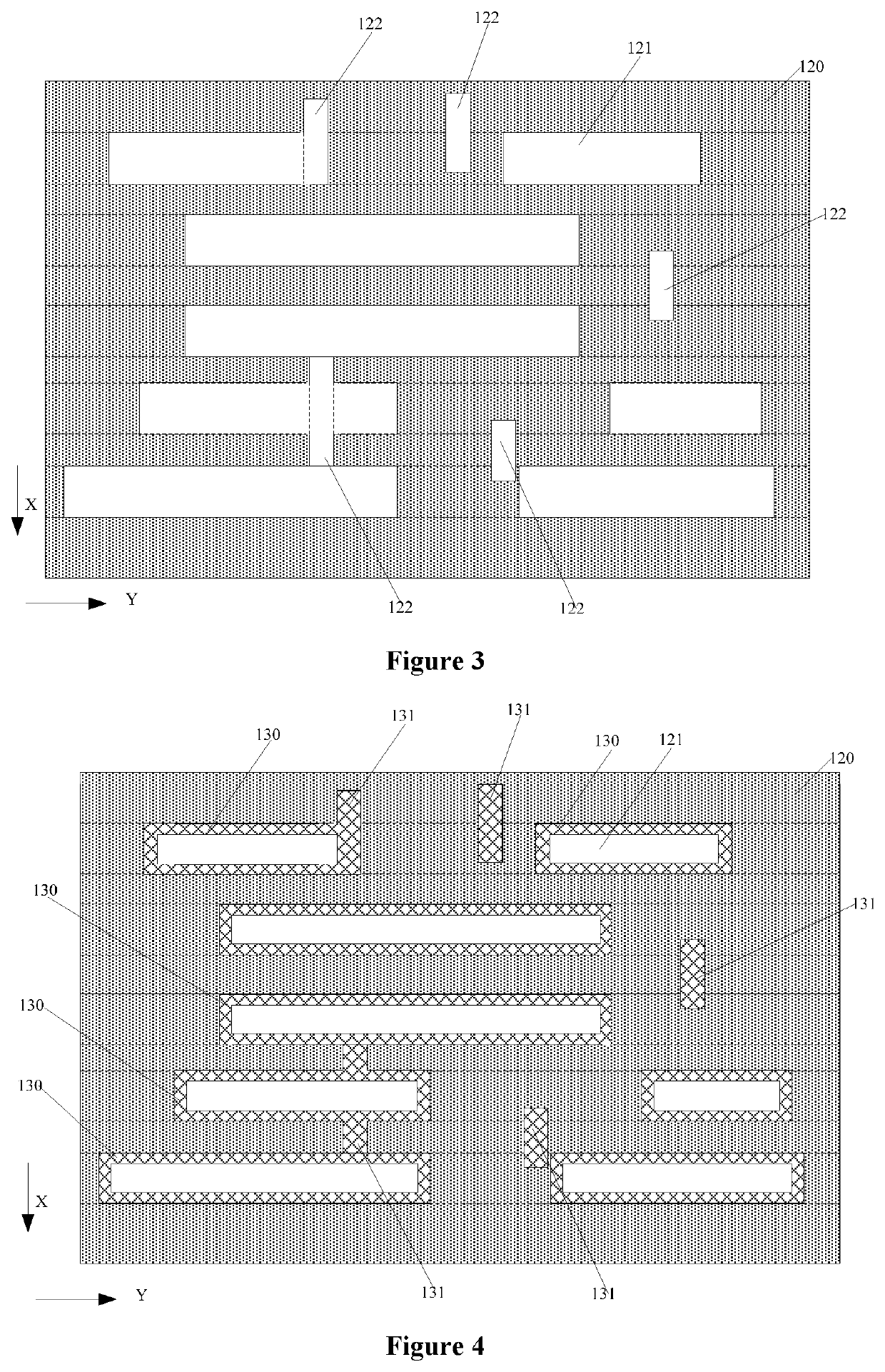
[0016]Referring to FIG. 2, a first mask layer 120 is formed over the first regions A01 and the second regions A02 of the layer 100 to-be-etched. A first trench 121 is formed in the first mask layer 120 over the first region A01.

[0017]Referring to FIG. 3, a divided trench 122 i...


PUM

PropertyMeasurementUnit
dielectric constantaaaaaaaaaa
sizeaaaaaaaaaa
sizeaaaaaaaaaa

Abstract

A semiconductor device and a method for forming the semiconductor device are provided. The method includes providing a layer to-be-etched including a first sub-trench region and a second sub-trench region. The method also includes forming a first mask layer over the layer to-be-etched and a second mask layer over the first mask layer, and forming a first sub-trench disposed over the first sub-trench region in the second mask layer. In addition, the method includes forming a first divided trench in the first mask layer and forming a second sub-trench disposed over the second sub-trench region in the second mask layer. Further, the method includes forming a first divided filling layer in the first divided trench, and forming a first middle trench in the first mask layer. The first divided filling layer divides the first middle trench in a second direction.

Description

CROSS-REFERENCES TO RELATED APPLICATIONS[0001]This application claims the priority of Chinese patent application No. 201910155842.7, filed on Mar. 1, 2019, the entirety of which is incorporated herein by reference.FIELD OF THE DISCLOSURE[0002]The present disclosure generally relates to the field of semiconductor manufacturing and, more particularly, relates to a semiconductor device and a fabrication method thereof.BACKGROUND[0003]In a semiconductor device manufacturing process, a pattern of a mask is often transferred to a substrate using a photolithography process. The photolithography process includes providing a substrate and forming a photoresist layer on the substrate. The photolithography process also includes exposing and developing the photoresist layer to form a patterned photoresist layer, such that the pattern of the mask is transferred to the photoresist layer. Further, the photolithography process includes etching the substrate by using the patterned photoresist layer ...

Claims


Application Information

Patent Timeline
Patent Type & Authority Applications(United States)
IPC IPC(8): H01L21/033H01L21/311H01L21/027H01L21/3105H01L21/768
CPCH01L21/31051H01L21/76816H01L21/0332H01L21/76877H01L21/0337H01L21/0274H01L21/31144H01L21/0334H01L21/0338
Inventor JIN, JISONGHE, ZEJUNNI, JIAWU, YANHUAPANG, JUNLING
Owner SEMICON MFG INT (SHANGHAI) CORP
Why Eureka
Try Eureka