
Electronic component

a technology of electronic components and components, applied in the field of electronic components, can solve the problems of leakage to the silicon substrate and loss increase, and achieve the effect of reducing or preventing the loss of the acoustic wave element 29

Active Publication Date: 2020-09-17
MURATA MFG CO LTD
View PDF2 Cites 2 Cited by
  • Summary
  • Abstract
  • Description
  • Claims
  • Application Information

AI Technical Summary

Benefits of technology

The present invention relates to an electronic component that includes a support member and a piezoelectric film. The support member has a high-impurity-concentration region and a low-impurity-concentration region. The low-impurity-concentration region is located where the energy of the acoustic wave is low, reducing leakage current and preventing loss of the acoustic wave element. The distance between the support member and the piezoelectric film is preferably about 40λ or more, and the thickness of the low-impurity-concentration region is preferably about 10λ or more and about 180 μm or less. The low acoustic velocity film is preferably made of silicon oxide, which has positive temperature characteristics and reduces the temperature dependence of the electronic component. The film thickness of the low acoustic velocity film is preferably about 2.0λ or less to reduce film stress and prevent warping of the wafer. The invention provides a composite device of the acoustic wave element and the semiconductor element while reducing or preventing loss of the acoustic wave element and achieving size reduction.

Problems solved by technology

Using a silicon substrate having low resistivity for an acoustic wave element including a piezoelectric film having a thickness of 3.5λ or less (λ is the wavelength of an acoustic wave determined by the electrode finger pitch of the interdigital transducer), there is a problem that the current which has to flow to the piezoelectric film leaks to the silicon substrate such that loss increases.

Method used


Image

  • Electronic component
  • Electronic component

Examples


Embodiment Construction

[0015]Electronic component according to preferred embodiments of the present invention will be described below with reference to the drawings.

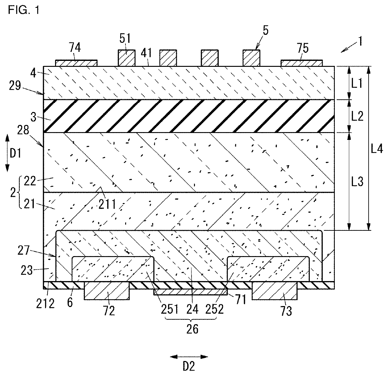
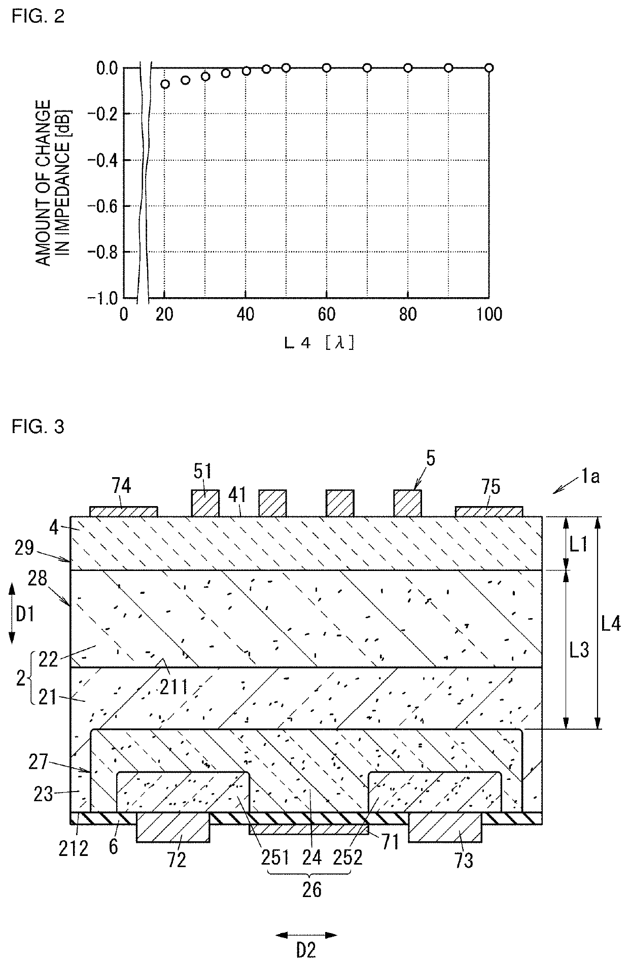
[0016]FIG. 1 and FIG. 3 described in the preferred embodiments and the like below are schematic drawings, and the size ratio and the thickness ratio of each element in the drawings are not limited to reflecting actual dimensional ratios.

(1) Overall Configuration of Electronic Component

[0017]Features of an electronic component according to a preferred embodiment of the present invention will be described with reference to the drawings.

[0018]As shown in FIG. 1, the electronic component 1 according to the present preferred embodiment includes a support member 2, a low acoustic velocity film 3, a piezoelectric film 4, and an interdigital transducer 5. In addition, the electronic component 1 includes an insulating film 6 and a plurality of electrodes. The support member 2 is a substrate including silicon as a primary component. The piezoelectric fi...


PUM

PropertyMeasurementUnit
thicknessaaaaaaaaaa
resistivityaaaaaaaaaa
thickness L3aaaaaaaaaa

Abstract

An electronic component includes a support member, a piezoelectric film, and an interdigital transducer. The support member includes silicon as a primary component. The piezoelectric film is provided directly or indirectly on the support member. The interdigital transducer includes a plurality of electrode fingers. The plurality of electrode fingers are provided side by side separately from each other. The interdigital transducer is provided on the principal surface of the piezoelectric film. The film thickness of the piezoelectric film is about 3.5λ or less, where λ denotes the wavelength of an acoustic wave determined by the electrode finger pitch of the interdigital transducer. In the support member, the high-impurity-concentration region is further from the piezoelectric film than the low-impurity-concentration region.

Description

CROSS REFERENCE TO RELATED APPLICATIONS[0001]This application claims the benefit of priority to Japanese Patent Application No. 2017-238931 filed on Dec. 13, 2017 and is a Continuation Application of PCT Application No. PCT / JP2018 / 043840 filed on Nov. 28, 2018. The entire contents of each application are hereby incorporated herein by reference.BACKGROUND OF THE INVENTION1. Field of the Invention[0002]The present invention generally relates to an electronic component and, in particular, to an electronic component including a piezoelectric film and an interdigital transducer.2. Description of the Related Art[0003]To date, acoustic wave devices (acoustic wave elements) including a piezoelectric film and an interdigital transducer have been known (see, for example, International Publication No. 2017 / 043427).[0004]In an acoustic wave device described in International Publication No. 2017 / 043427, a low acoustic velocity film, a piezoelectric film, and an interdigital transducer are stacke...

Claims


Application Information

Patent Timeline
Patent Type & Authority Applications(United States)
IPC IPC(8): H03H9/02H03H9/145H03H9/13H10N30/853H10N30/87H10N30/88
CPCH03H9/02228H03H9/14541H03H9/02566H03H9/131H01L25/065H01L25/07H01L25/18H03H9/0552H03H9/0557H03H9/02574H10N30/87H10N30/88H10N30/853
Inventor KOYANAGI, TAKUYAIWAMOTO, HIDEKI
Owner MURATA MFG CO LTD
Learn More