Illuminance sensor, electronic machine and 2d image sensor

a technology of illumination sensor and electronic machine, applied in the direction of polarising element, radio frequency control device, instruments, etc., can solve the problems of easy noise caused by illuminance sensor, difficult to dispose of illuminance sensor at a portion separated from the display portion, and narrow width of the so-called border portion around the display portion, etc., to achieve the effect of reducing undesirable influences

Active Publication Date: 2020-11-12
ROHM CO LTD
View PDF0 Cites 0 Cited by
  • Summary
  • Abstract
  • Description
  • Claims
  • Application Information

AI Technical Summary

Benefits of technology

[0006]The present invention is conceived of on the basis of the situations above, and aims to provide an illuminance sensor configurable in a narrow space and capable of mitigating undesirable influences caused by infrared light, and an electronic machine and a two-dimensional image sensor using the same.

Problems solved by technology

However, in a recent thin display device using an organic light-emitting diode (OLED) panel, the width of the so-called border portion around a display portion tends to become extremely narrow.
As a result, it may be difficult to dispose an illuminance sensor at a portion separated from the display portion, which is also undesirable from design perspectives.
Further, it is commonly considered that an illuminance sensor may easily produce noise caused by infrared light.
For example, smartphones and tablet terminals are commonly used outdoors, and such noise caused by infrared light becomes obstacles in sensing the brightness of the surrounding environment.

Method used


Image

  • Illuminance sensor, electronic machine and 2d image sensor
  • Illuminance sensor, electronic machine and 2d image sensor
  • Illuminance sensor, electronic machine and 2d image sensor

Examples


first embodiment

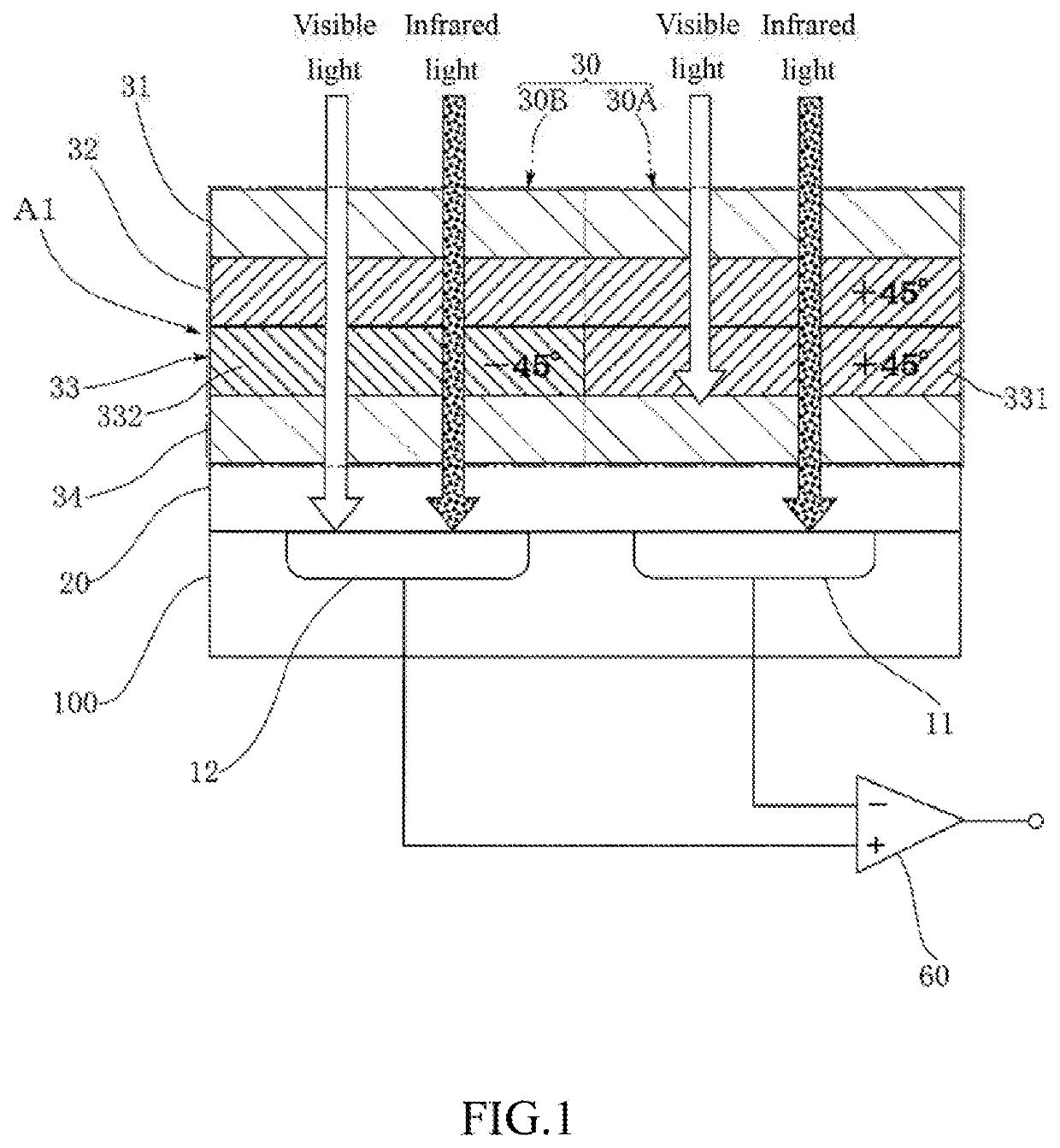
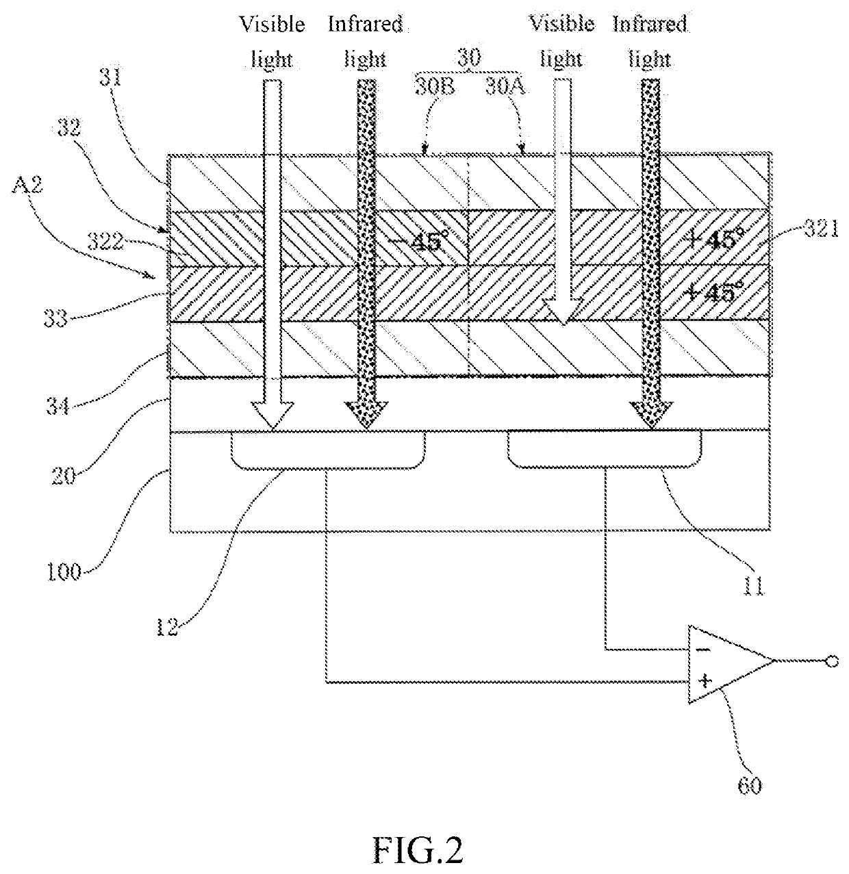
[0023]FIG. 1 shows an illuminance sensor according to the present invention, that is, an illuminance sensor A1. The illuminance sensor A1 includes a first light receiving portion 11, a second light receiving portion 12, an optical region 30, and a difference detecting portion 60.

[0024]The first light receiving portion 11 and the second light receiving portion 12 are, for example, photodiodes manufactured and incorporated into the same integrated circuit (IC), and are located in a same plane serving as the main surface of the IC 100. The optical region 30 is disposed opposite to the first light receiving portion 11 and the second light receiving portion 12. The optical region 30 has a first optical region 30A disposed corresponding to the first light receiving portion 11, and a second optical region 30B disposed corresponding to the second light receiving portion 12.

[0025]The optical region 30 (the first optical region 30A and the second optical region 30B) includes a first linear po...

second embodiment

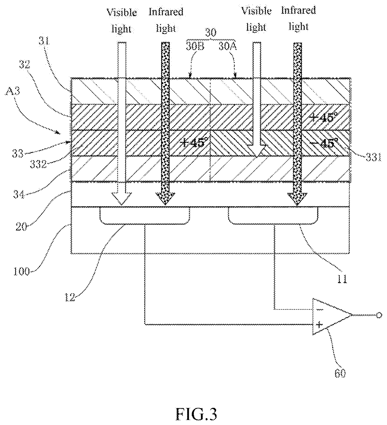
[0065]FIG. 3 shows an illuminance sensor A3 as an illuminance sensor according to the present invention. Compared to the illuminance sensor A1 in FIG. 1, the illuminance sensor A3 differs in terms of the relation of the polarization directions of the first linear polarization plate 31 and the second linear polarization plate 34, and the arrangements and configurations of the first quarter-wave plate 32 and the second quarter-wave plate 33, and the remaining configuration details are identical to those in the illuminance sensor A1 in FIG. 1. That is to say, in the illuminance sensor A3 in FIG. 3, the polarization direction (the first polarization direction) of the first linear polarization plate 31 differs from the polarization direction (the second polarization direction) of the second linear polarization plate 34 by 90°. In FIG. 3, slant shading lines in different directions are used for representation. The first quarter-wave plate 32 is set to “+45°” in the entire of the first opt...

third embodiment

[0101]FIG. 5 shows an illuminance sensor according to the present invention. The illuminance sensor A5 shown in the drawing primary differs from the illuminance sensors A1 to A4 by the configurations of the first light receiving portion 11 and the second light receiving portion 12 and the configuration of the color filter layer 20. Further, in FIG. 5, only the second linear polarization plate 34 in the optical region 30 (the first optical region 30A and the second optical region 30B) is depicted, and the first linear polarization plate 31, the first quarter-wave plate 32 and the second quarter-wave plate 33 are omitted.

[0102]In the illuminance sensor A5 of this embodiment, the first light receiving portion 11 and the second light receiving portion 12 includes a plurality of light receiving elements, respectively. More specifically, the first light receiving portion 11 includes a first light receiving element 111, a second light receiving element 112 and a third light receiving eleme...


PUM


Abstract

In an illuminance sensor, a slow axis of a first quarter-wave plate has a relation of +45° or −45° in regard to a polarization direction of a first linear polarization plate; a relation of a slow axis of a first portion of a second quarter-wave plate in regard to a polarization direction of a second linear polarization plate is the same with relation of the slow axis of the first quarter-wave plate in regard to the polarization direction of the first linear polarization plate, that is, +45° or −45°; and a relation of a slow axis of a second portion of the second quarter plate in regard to the polarization direction of the second linear polarization plate is −45° or +45° that is opposite in sign to the relation of the slow axis of the first quarter-plate in regard to the polarization direction of the first linear polarization plate.

Description

BACKGROUND OF THE INVENTIONField of the Invention[0001]The present invention relates to an illuminance sensor, and an electronic machine and a two-dimensional (2D) image sensor having the same.Description of the Prior Art[0002]For example, as disclosed in patent document 1, an illuminance sensor sensing ambient brightness is sometimes provided in a display device in order to control display brightness.[0003]In such display device, an illuminance sensor is usually separated from a display portion and is disposed at an appropriate position of a frame. However, in a recent thin display device using an organic light-emitting diode (OLED) panel, the width of the so-called border portion around a display portion tends to become extremely narrow. As a result, it may be difficult to dispose an illuminance sensor at a portion separated from the display portion, which is also undesirable from design perspectives. On the other hand, in order to control the display brightness of a display devic...

Claims


Application Information

Patent Timeline
Patent Type & Authority Applications(United States)
IPC IPC(8): H01L31/0232H01L31/09G02B5/30H01L27/32H01L27/146
CPCH01L31/02327H01L27/3227H01L27/14621G02B5/3066H01L31/09H01L27/14625H01L31/02024H01L27/14605G02B5/201G02B5/208G02B5/223H10K59/65H10K50/86H01L31/02162H01L31/101H10K59/60
Inventor UEDAIRA, YOSHITSUGU
Owner ROHM CO LTD
Why Eureka
Try Eureka