Semiconductor package and manufacturing method thereof

Active Publication Date: 2020-11-19
POWERTECH TECHNOLOGY
View PDF0 Cites 7 Cited by
  • Summary
  • Abstract
  • Description
  • Claims
  • Application Information

AI Technical Summary

Benefits of technology

[0003]Accordingly, the present disclosure provides a semiconductor package and a manufacturing method thereof, which is less susceptible to the warpage problem.
[0024]As above, the semiconductor package according to embodiments in the present disclosure includes at least one semiconductor die, which is laterally encapsulated by an encapsulant. A redistribution layer is disposed at an active side of the semiconductor die and a front surface of the encapsulant, whereas a polymer pattern is formed at a back surface of the encapsulant. As such, the encapsulant is located between the redistribution layer and the polymer pattern. A coefficient of thermal expansion (CTE) of the encapsulant may be greater than or less than the CTEs of the polymer pattern and the dielectric layers in the redistribution layer. Thereby, the stress caused by the CTE mismatch between the encapsulant and the dielectric layers can be at least partially cancelled by the stress caused by the CTE mismatch between the encapsulant and the polymer pattern. Accordingly, total stress in the semiconductor package can be reduced, and the semiconductor package may be less susceptible to warpage. Furthermore, the polymer pattern is formed over a portion of the encapsulant surrounding the semiconductor die, and can be regarded as having an opening overlapped with the semiconductor die. In this way, a heat dissipation structure covering the polymer pattern can be in physical contact with the semiconductor die. Therefore, heat generated by the semiconductor dies can be more effectively dissipated through the heat dissipation structure.

Problems solved by technology

However, during manufacturing process, fan-out semiconductor package is often subjected to a high level stress, and such stress may result in warpage issues.

Method used


Image

  • Semiconductor package and manufacturing method thereof
  • Semiconductor package and manufacturing method thereof
  • Semiconductor package and manufacturing method thereof

Examples


Embodiment Construction

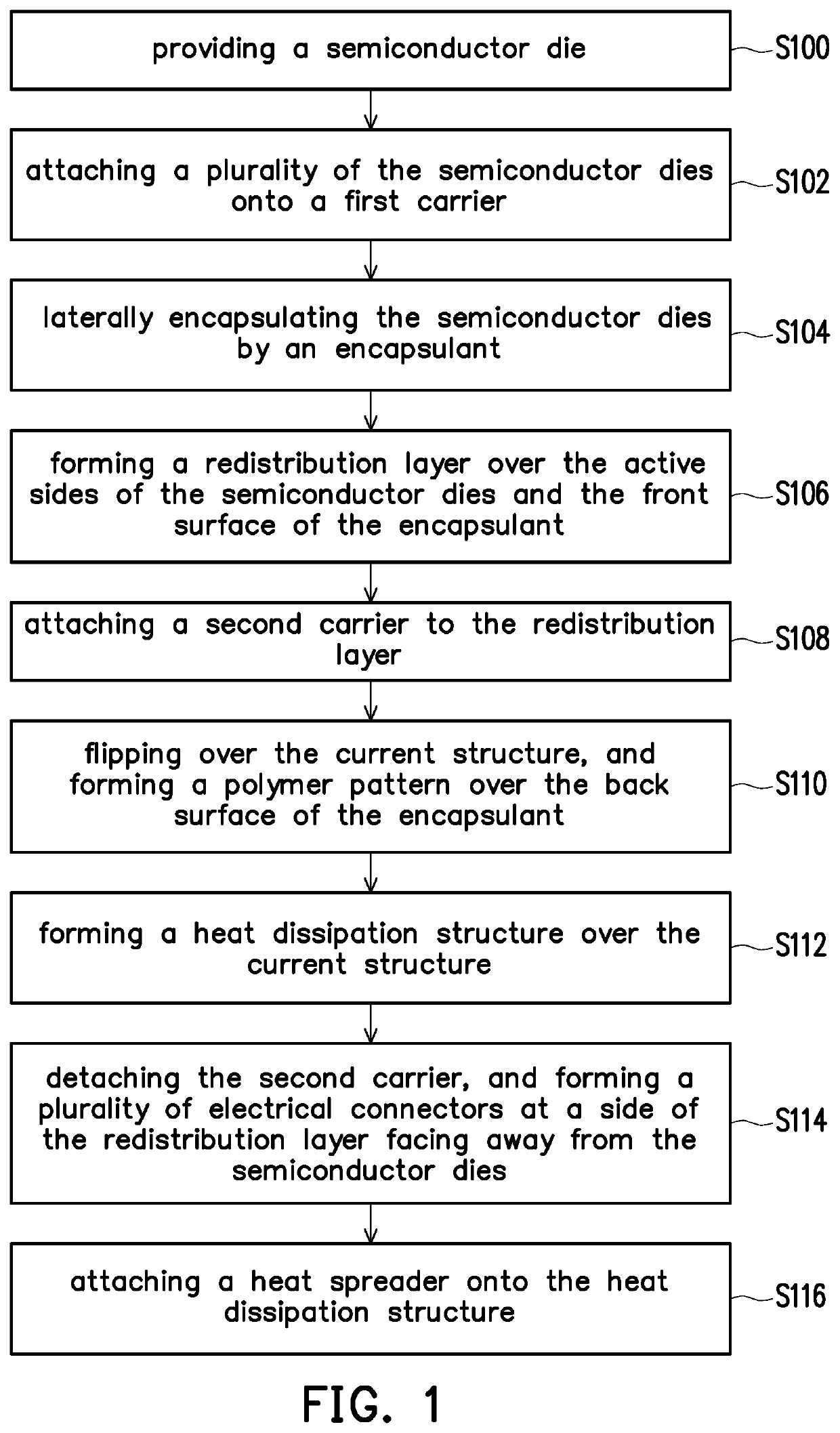
[0034]FIG. 1 is a process flow chart illustrating a manufacturing method of a semiconductor package according to some embodiments of the present disclosure. FIG. 2A through FIG. 2I are cross-sectional views illustrating structures at various stages during the manufacturing process of the semiconductor package according to some embodiments of the present disclosure.

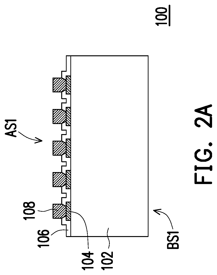
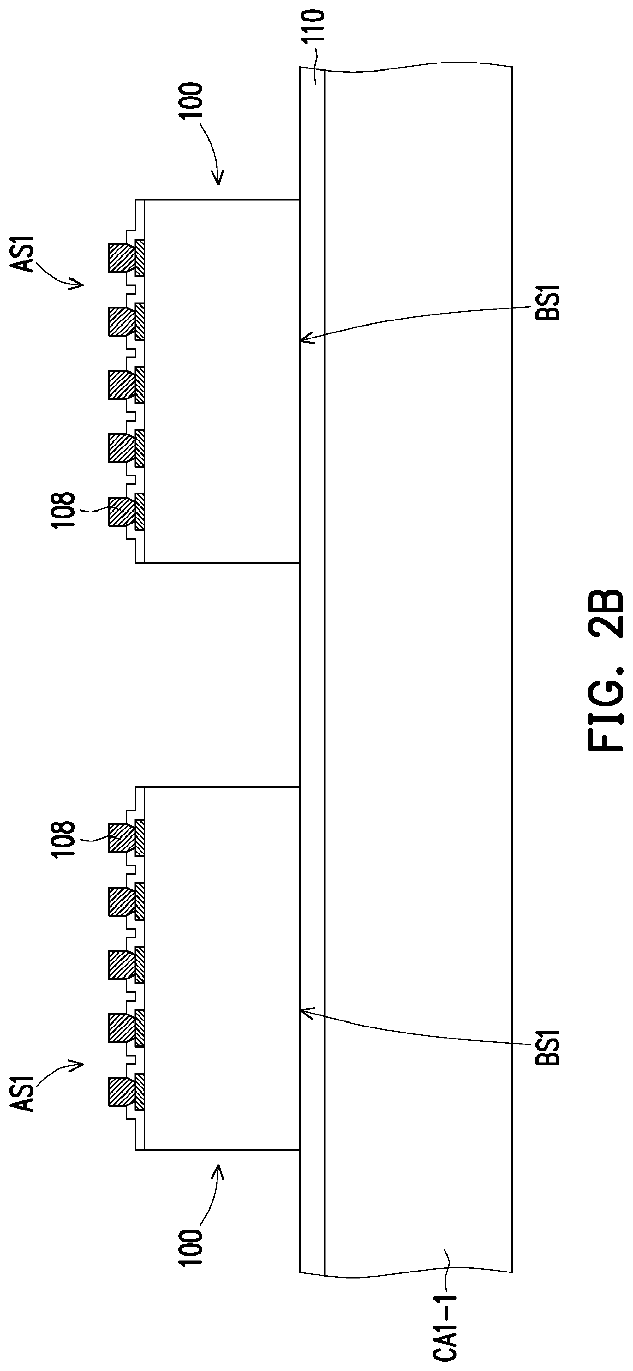
[0035]Referring to FIG. 1 and FIG. 2A, step S100 is performed, and a semiconductor die 100 is provided. The semiconductor die 100 may be a semiconductor die singulated from a device wafer. In some embodiments, the semiconductor die 100 may be a logic integrated circuit (IC) die, a memory IC die (e.g., a dynamic random access memory (DRAM) die), a system-on-chip (SOC) die, an analog IC die, an application-specific IC (ASIC) die, or the like. The semiconductor die 100 includes a semiconductor substrate 102, which may be a portion of a semiconductor wafer or a semiconductor-on-insulator (SOI) wafer. A plurality of electronic ...


PUM

PropertyMeasurementUnit
heat dissipationaaaaaaaaaa
thicknessaaaaaaaaaa
conductiveaaaaaaaaaa

Abstract

A semiconductor package and a manufacturing method thereof are provided. The semiconductor package includes a semiconductor die, an encapsulant, a redistribution layer, a polymer pattern and a heat dissipation structure. The semiconductor die has conductive pads at its active side, and is laterally encapsulated by the encapsulant. The redistribution layer is disposed at the active side of the semiconductor die, and spans over a front surface of the encapsulant. The redistribution layer is electrically connected with the conductive pads. The polymer pattern is disposed at a back surface of the encapsulant that is facing away from the front surface of the encapsulant. The semiconductor die is surrounded by the polymer pattern. The heat dissipation structure is in contact with a back side of the semiconductor die that is facing away from the active side, and extends onto the polymer pattern.

Description

BACKGROUNDTechnical Field[0001]The present disclosure relates to a semiconductor package and a manufacturing method thereof, and more particularly, to a fan-out semiconductor package and a manufacturing method thereof.Description of Related Art[0002]Fan-out semiconductor packaging is a packaging process in which contacts of a semiconductor die are redistributed over a larger area through a redistribution layer, and provides a solution for packaging semiconductor devices that require higher integration level and greater number of external contacts. However, during manufacturing process, fan-out semiconductor package is often subjected to a high level stress, and such stress may result in warpage issues.SUMMARY[0003]Accordingly, the present disclosure provides a semiconductor package and a manufacturing method thereof, which is less susceptible to the warpage problem.[0004]According to some embodiments, a semiconductor package includes a semiconductor die, an encapsulant, a redistribu...

Claims


Application Information

Patent Timeline
Patent Type & Authority Applications(United States)
IPC IPC(8): H01L23/433H01L23/31H01L23/498H01L23/367H01L23/00H01L21/56H01L21/48H01L23/538
CPCH01L23/49838H01L23/3128H01L21/568H01L23/433H01L23/49822H01L23/49816H01L23/3135H01L21/481H01L21/4857H01L2224/16227H01L23/5383H01L23/3672H01L24/16H01L23/36H01L23/5389H01L2224/13082H01L24/19H01L24/20H01L2924/181H01L2924/15311H01L2224/73204H01L2224/32225H01L2224/16225H01L2224/26175H01L2224/83007H01L2924/18161H01L2924/15174H01L24/32H01L24/13H01L24/81H01L24/29H01L2224/92125H01L24/73H01L2224/8385H01L24/97H01L2224/81801H01L2224/81001H01L21/6835H01L24/83H01L24/92H01L2224/2929H01L2224/29298H01L2221/68345H01L2221/68372H01L21/561H01L21/56H01L2924/00012
Inventor HUANG, KUN-YUNG
Owner POWERTECH TECHNOLOGY
Why Eureka
Try Eureka