Eureka AIR delivers breakthrough ideas for toughest innovation challenges, trusted by R&D personnel around the world.

Array substrate and display panel

Pending Publication Date: 2021-06-10
SHENZHEN CHINA STAR OPTOELECTRONICS SEMICON DISPLAY TECH CO LTD
View PDF5 Cites 1 Cited by
  • Summary
  • Abstract
  • Description
  • Claims
  • Application Information

AI Technical Summary

Benefits of technology

The present invention provides an array substrate and a display panel that solves the problem of current display panels not being able to identify alignment identification terminals due to limited space in the frame regions. The technical effect of the invention is that it provides an array substrate with an alignment identification terminal that is at least partially disposed in a sub-pixel electrode region, allowing for better identification and alignment during manufacturing processes. This improves the manufacturing process of display panels and ensures that they can identify and align with external devices.

Problems solved by technology

However, for display panels with ultra-narrow frames (a width of the frame is less than 1 mm), there is insufficient space in the frame regions, and arrangements of the alignment identification terminals are limited, which will cause risks that charge-coupled device (CCD) camera will not identify them.
Therefore, current display panels have problems that alignment identification terminals cannot be identified, and thus needs to be solved.

Method used


Image

  • Array substrate and display panel
  • Array substrate and display panel
  • Array substrate and display panel

Examples


Embodiment Construction

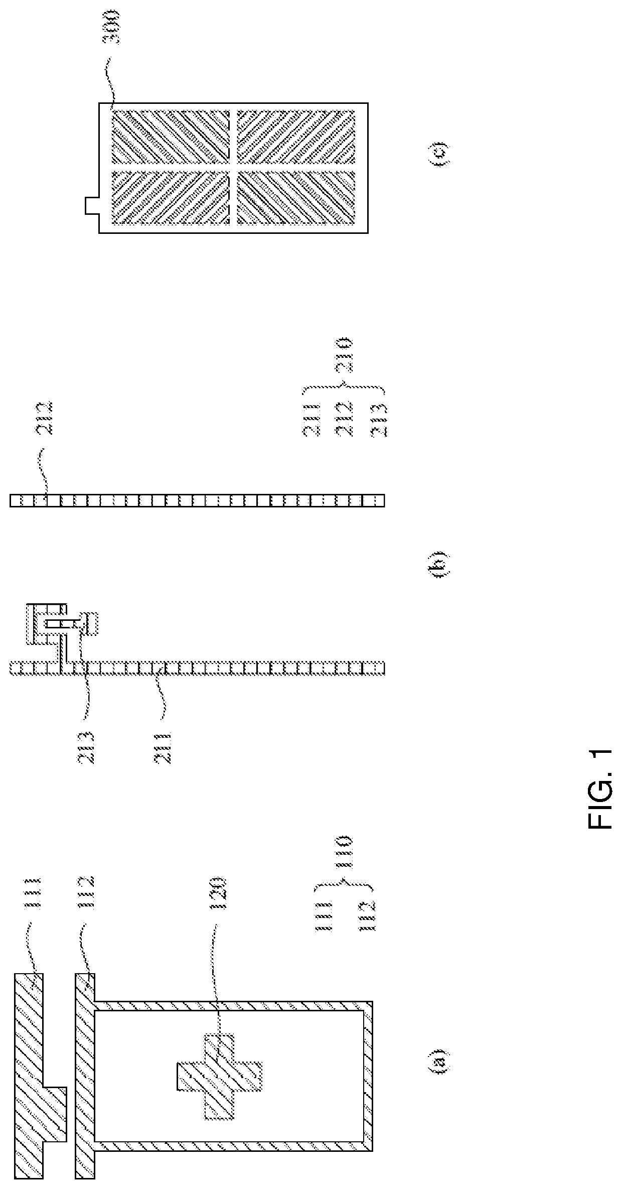
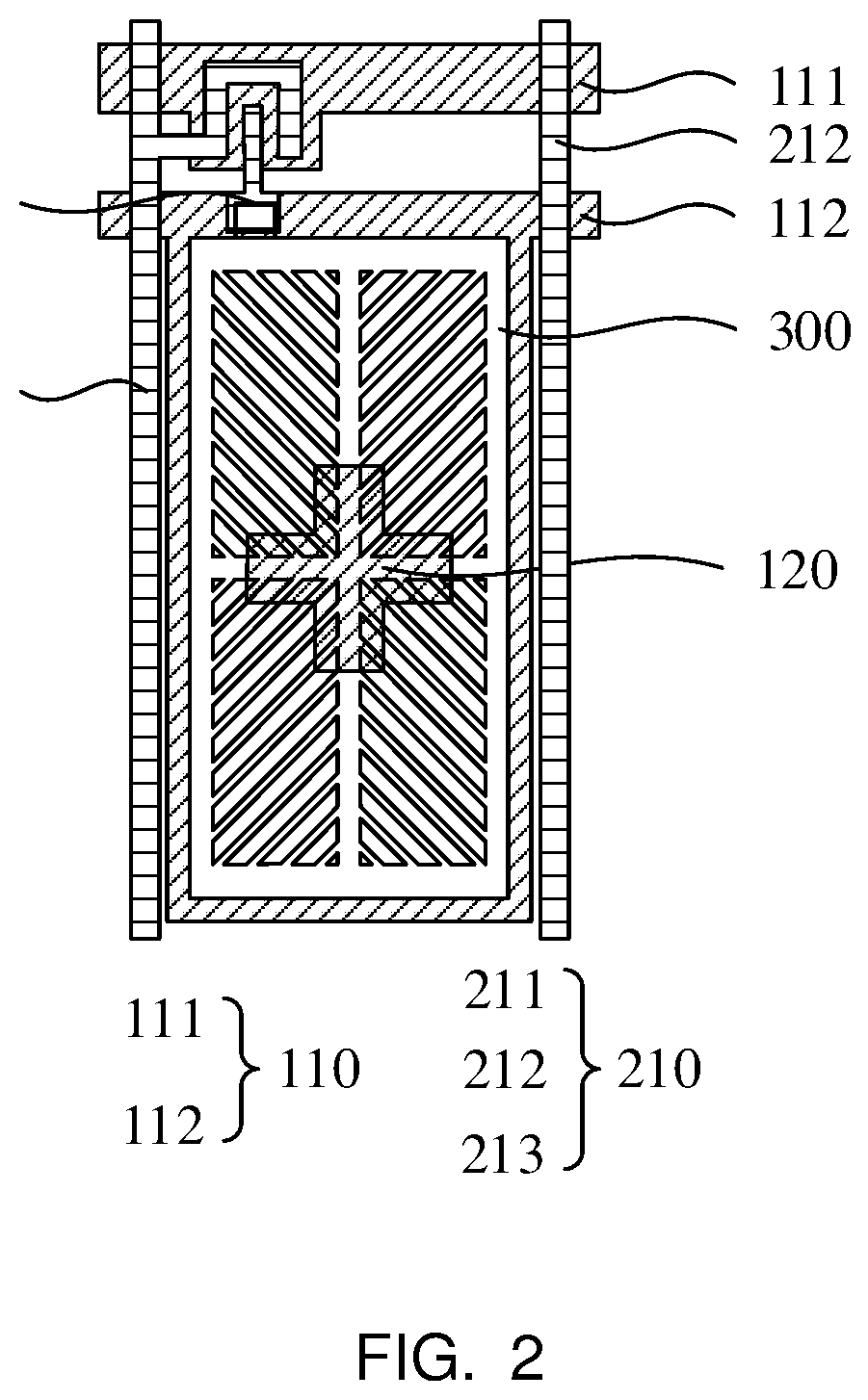
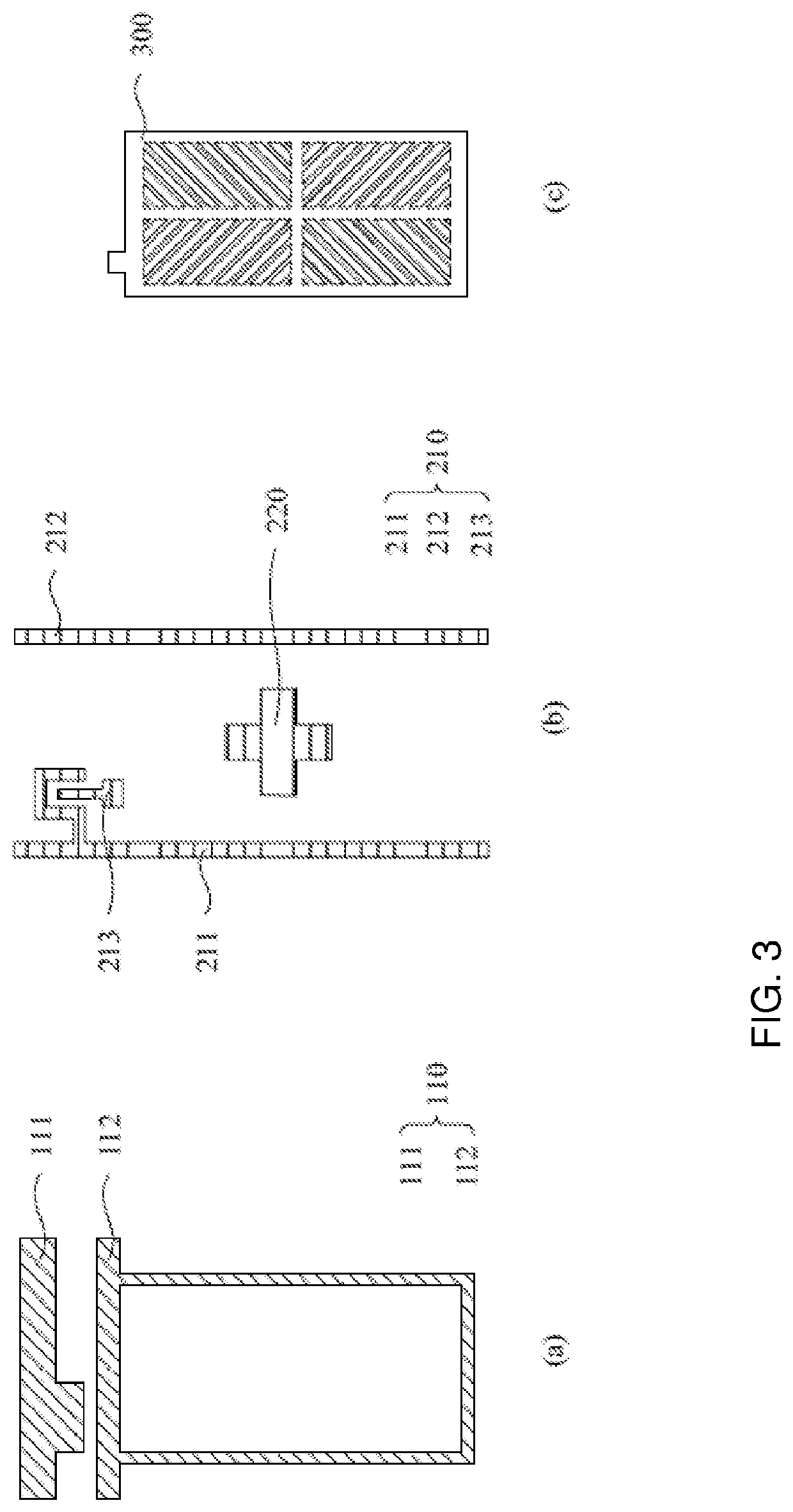
[0058]The following description of the various embodiments is provided with reference to the accompanying drawings. Directional terms, such as upper, lower, front, back, left, right, inner, outer, and lateral side, mentioned in the present invention are only for reference. Therefore, the directional terms are used for describing and understanding rather than limiting the present invention. In the figures, units having similar structures are used for the same reference numbers.

[0059]The present invention provides an array substrate to alleviate a problem that current display panels do not identify alignment identification terminals.

[0060]In an embodiment, the array substrate provided in the present invention comprises:

[0061]a base;

[0062]a first metal layer formed on the base;

[0063]a second metal layer formed on the first metal layer;

[0064]a pixel electrode layer formed on the second metal layer, wherein the pixel electrode layer is patterned to form a pixel electrode, and the pixel e...


PUM


Abstract

The present invention provides an array substrate and a display panel. The array substrate includes a substrate, a first metal layer, a second metal layer, a pixel electrode layer, and an alignment identification terminal that are sequentially stacked. The alignment identification terminal is disposed in at least one of the first metal layer and the second metal layer, and is at least partially disposed in a sub-pixel electrode region. An arrangement of the alignment identification terminal is no longer limited by a narrow frame, and a size can be made larger to meet the needs of a CCD identification, ensuring an accuracy of identification and alignment.

Description

FIELD OF INVENTION[0001]The present invention relates to the field of displays, and in particular, to an array substrate and a display panel.BACKGROUND OF INVENTION[0002]In manufacturing processes of display panels, alignment identification terminals are mainly used for alignments of machines and substrates.[0003]In conventional designs, the alignment identification terminals are disposed outside display regions of the display panels and within frame regions. However, for display panels with ultra-narrow frames (a width of the frame is less than 1 mm), there is insufficient space in the frame regions, and arrangements of the alignment identification terminals are limited, which will cause risks that charge-coupled device (CCD) camera will not identify them.[0004]Therefore, current display panels have problems that alignment identification terminals cannot be identified, and thus needs to be solved.Technical Problem[0005]The present invention provides an array substrate and a display...

Claims


Application Information

Patent Timeline
IPC IPC(8): H01L23/544H01L27/12
CPCH01L23/544H01L2223/5442H01L2223/54426H01L27/124H01L2223/54486
Inventor LIU, LINFENGTANG, AIHUAYE, YANXIYANG, CHIHMINGLIN, YUNGLUN
Owner SHENZHEN CHINA STAR OPTOELECTRONICS SEMICON DISPLAY TECH CO LTD
Why Eureka
Eureka Blog
Learn More