Double-sided display panel and display device
a display panel and display device technology, applied in semiconductor devices, identification means, instruments, etc., can solve the problems of increasing the cost of a display system and complicated structure of a display device, and achieve the effects of reducing the number of bindings and complexity, reducing the structural complexity of a display device, and reducing the weight of the display devi
- Summary
- Abstract
- Description
- Claims
- Application Information
AI Technical Summary
Benefits of technology
Problems solved by technology
Method used
Image
Examples
embodiment 1
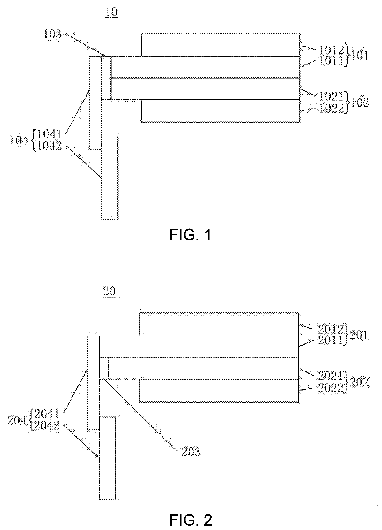
[0036]Referring to FIG. 1, the double-sided display panel 10 includes a first display module 101, a second display module 102, a conductive layer 103, and a driving module 104. The first display module 101 and the second display module 102 are disposed opposite to each other.
[0037]The first display module 101 includes a first thin film transistor substrate 1011 and a first color filter substrate 1012, which are disposed opposite to each other. The second display module 102 includes a second thin film transistor substrate 1021 and a second color filter substrate 1022, which are disposed opposite to each other. The first thin film transistor substrate 1011 is attached to the second thin film transistor substrate 1021. The first color filter substrate 1012 and the second color filter substrate 1022 are opposite to each other across the first thin film transistor substrate 1011 and the second thin film transistor substrate 1021.
[0038]It can be noted that the first display module 101 and...
embodiment 2
[0046]Referring to FIG. 2, the double-sided display panel 20 includes a first display module 201, a second display module 202, a conductive layer 203, and a driving module 204. The first display module 201 and the second display module 202 are disposed opposite to each other.
[0047]The first display module 201 includes a first thin film transistor substrate 2011 and a first color filter substrate 2012, which are disposed opposite to each other. The second display module 202 includes a second thin film transistor substrate 2021 and a second color filter substrate 2022, which are disposed opposite to each other. The first thin film transistor substrate 2011 is attached to the second thin film transistor substrate 2021. The first color filter substrate 2012 and the second color filter substrate 2022 are opposite to each other across the first thin film transistor substrate 2011 and the second thin film transistor substrate 2021.
[0048]It can be noted that the first display module 201 and...
embodiment 3
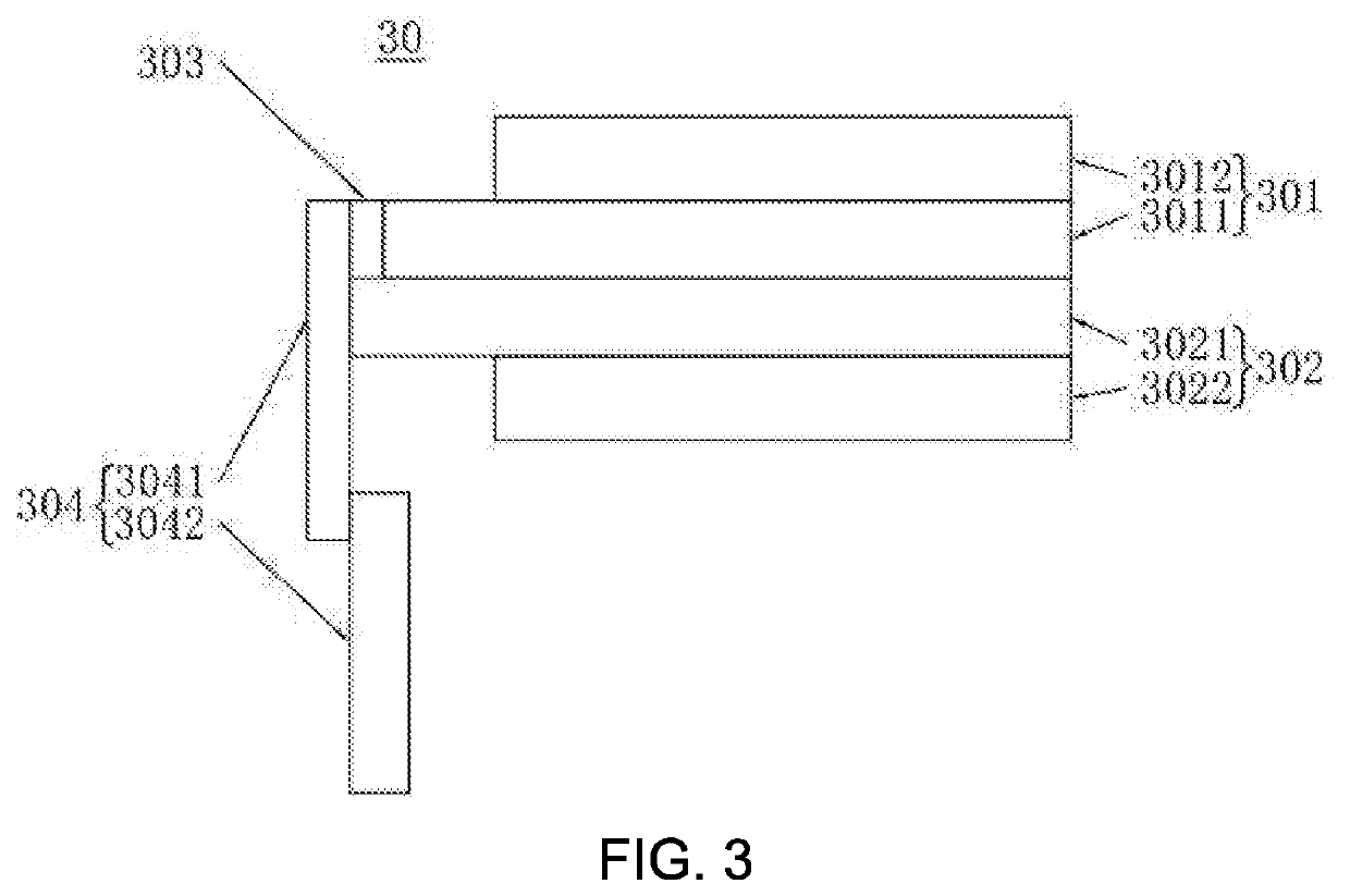
[0056]Referring to FIG. 3, the double-sided display panel 30 includes a first display module 301, a second display module 302, a conductive layer 303, and a driving module 304. The first display module 301 and the second display module 302 are disposed opposite to each other.
[0057]The first display module 301 includes a first thin film transistor substrate 3011 and a first color filter substrate 3012, which are disposed opposite to each other. The second display module 302 includes a second thin film transistor substrate 3021 and a second color filter substrate 3022, which are disposed opposite to each other. The first thin film transistor substrate 3011 is attached to the second thin film transistor substrate 3021. The first color filter substrate 3012 and the second color filter substrate 3022 are opposite to each other across the first thin film transistor substrate 3011 and the second thin film transistor substrate 3021.
[0058]It can be noted that the first display module 301 and...
PUM
| Property | Measurement | Unit |
|---|---|---|
| conductive | aaaaa | aaaaa |
| thickness | aaaaa | aaaaa |
| time | aaaaa | aaaaa |
Abstract
Description
Claims
Application Information

