
Power Semiconductor Device with Free-Floating Packaging Concept

Pending Publication Date: 2021-12-09
HITACHI ENERGY SWITZERLAND AG
View PDF0 Cites 0 Cited by
  • Summary
  • Abstract
  • Description
  • Claims
  • Application Information

AI Technical Summary

Benefits of technology

[0012]In view of the above disadvantages in the prior art it is an object of the invention to provide a power semiconductor device in which heat dissipation is effic

Problems solved by technology

However, bonding the molybdenum disk to the semiconductor wafer involves the risk to generate conductive particles on the wafer in the area of the junction termination and increases the manufacturing costs.
This results in a relatively bad removal of heat generated in the circumferential edge region of the wafer which is not in contact with the molybdenum disks.
As for the a

Method used


Image

  • Power Semiconductor Device with Free-Floating Packaging Concept
  • Power Semiconductor Device with Free-Floating Packaging Concept
  • Power Semiconductor Device with Free-Floating Packaging Concept

Examples


Example

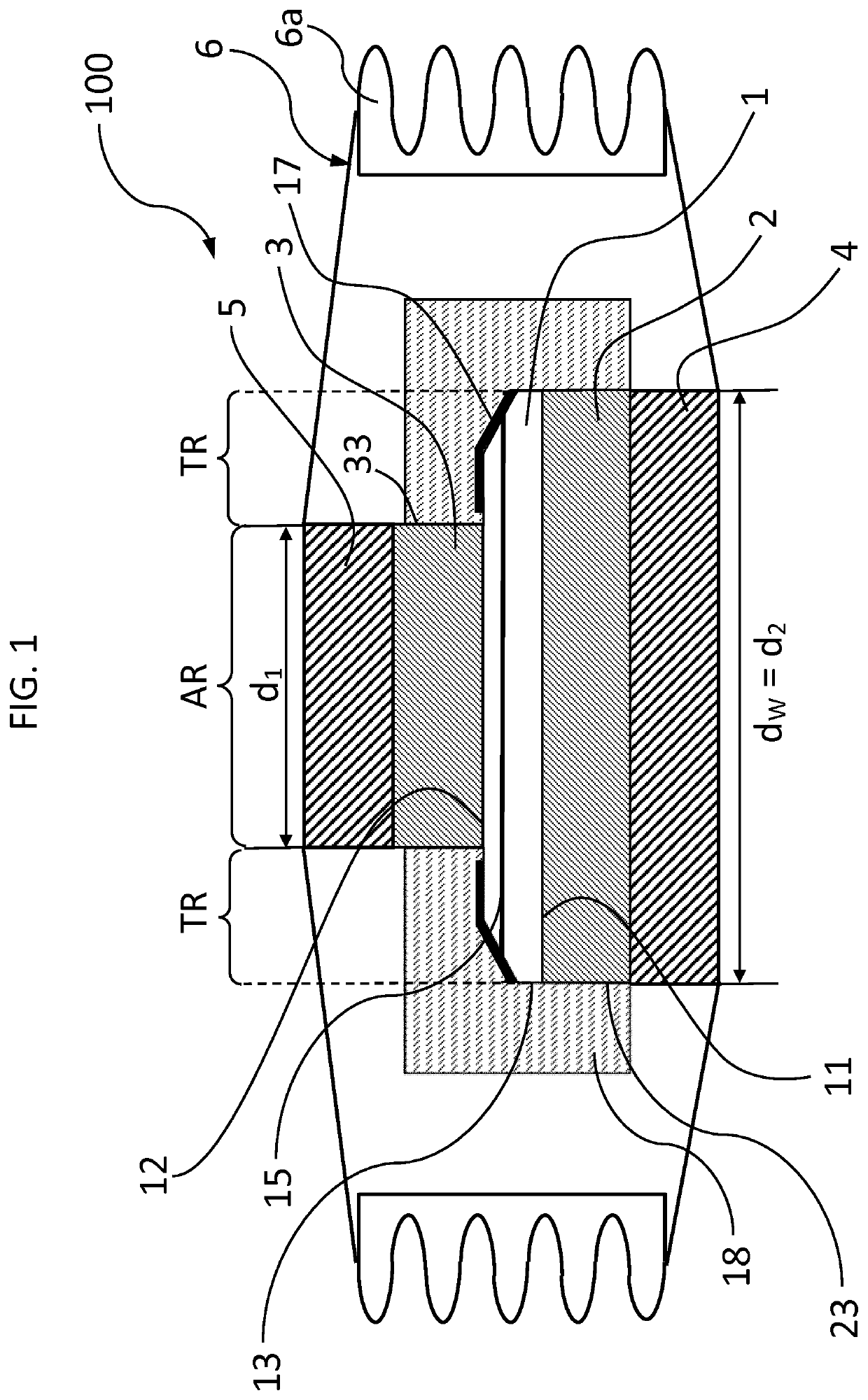
[0036]In the following a power semiconductor device 100 according to a first embodiment is described with reference to FIG. 1. The power semiconductor device 100 according to the first embodiment is a press-pack type device comprising a semiconductor wafer 1, a first metal disk 2, a second metal disk 3, a first pole piece 4, a second pole piece 5 and a housing 6. The semiconductor wafer 1 has a first main side 11, a second main side 12 opposite to the first main side 11, and a lateral side 13 connecting the first main side 11 and the second main side 12.

[0037]In an orthogonal projection onto a plane parallel to the first main side 11, the semiconductor wafer 1 has an active region AR in a central area of the semiconductor wafer 1 and a junction termination region TR that extends along a circumferential edge of the semiconductor wafer 1 to laterally surround the active region AR. Therein, any direction parallel to the first main side is a lateral direction. At least one junction 15 i...

Example

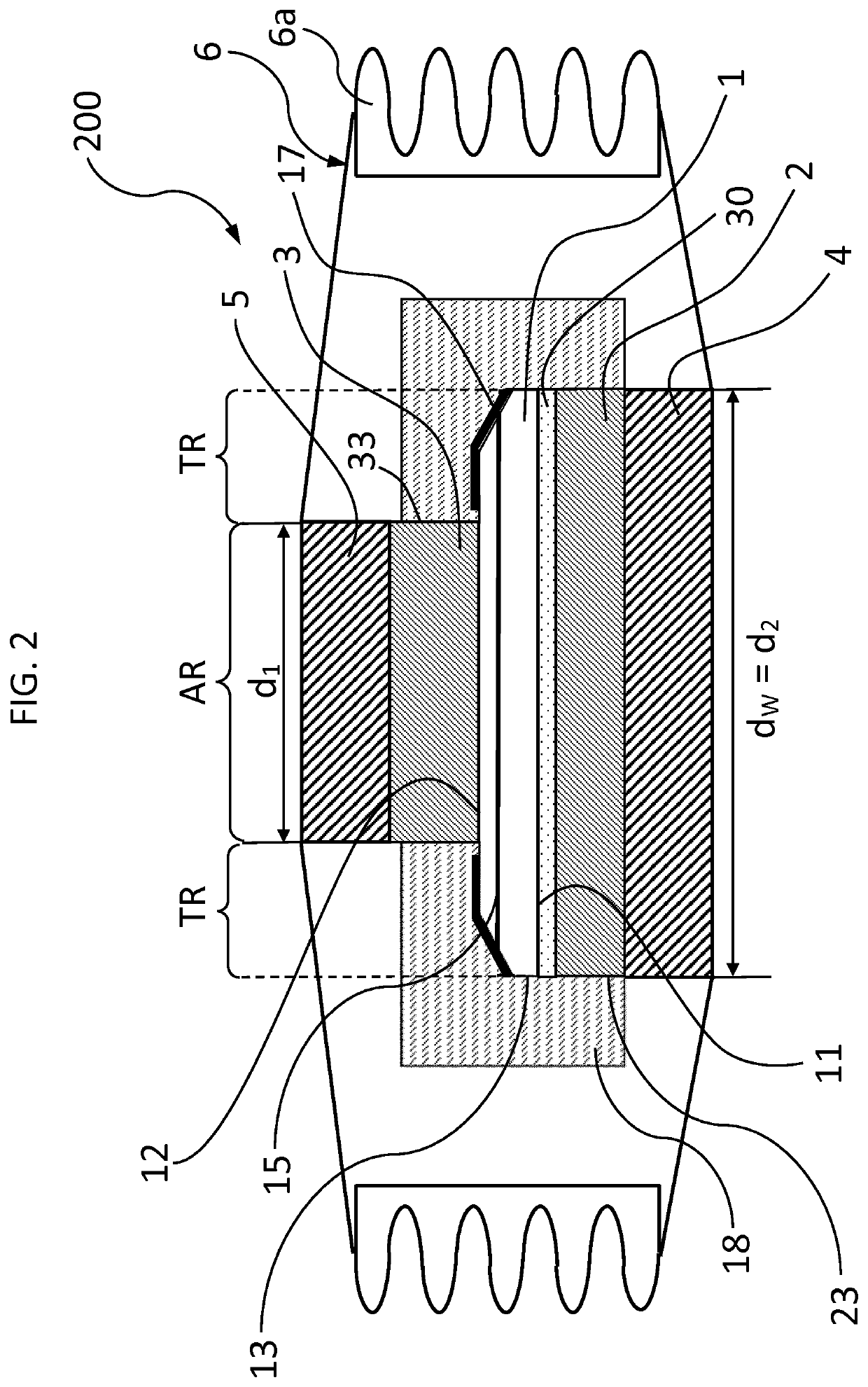
[0044]In the following a power semiconductor device 200 according to a second embodiment is described with reference to FIG. 2. Due to the many similarities between the first and the second embodiment, only differences between these two embodiments will be described. With regard to all other features it is referred to the above discussion of the first embodiment. In particular, elements having the same reference sign shall refer to elements having the same characteristics and features as the elements described above for the first embodiment. The power semiconductor device 200 according to the second embodiment differs from that according to the first embodiment in that a metal layer 30 is sandwiched between the first metal disk 2 and the semiconductor wafer 1, the metal layer 30 having a melting point below 150° C., exemplarily below 125° C., more exemplarily below 100° C. The metal layer 30 may include any one of Liquid Metal Thermal Interfaces (LMTI). It can be an eutectic alloy b...

Example

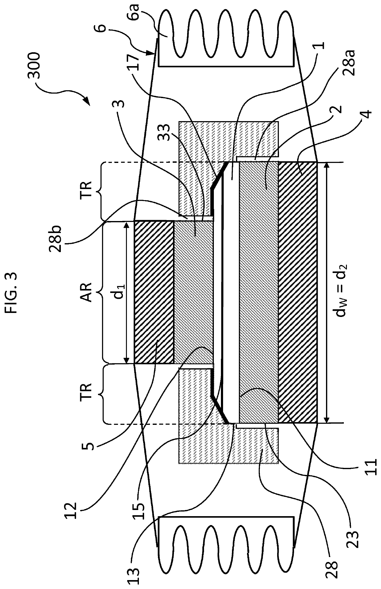
[0045]In the following a power semiconductor device 300 according to a third embodiment is described with reference to FIG. 3. Due to the many similarities between the first and the third embodiment, only differences between these two embodiments will be described in the following. With regard to all other features it is referred to the above discussion of the first embodiment. The power semiconductor device 300 differs from the power semiconductor device 200 in that first metal disk 2 is not fixed or glued to the semiconductor wafer 1 by the protection layer 28. Accordingly, the protection layer 28 differs from the protection layer 18 in that it is not fixed or glued to the lateral side surface 23 of the first metal disk 2. In FIG. 3 this difference is reflected by a gap 28a between the lateral side surface 23 of the first metal disk 2 and the protection layer 28. Likewise, in contrast to the power semiconductor device 100, the protection layer 28 is also not fixed or glued to the ...


PUM


Abstract

A power semiconductor device includes a semiconductor wafer having a junction and a junction termination laterally surrounding the junction. A protection layer covers the lateral side of the semiconductor wafer and covers the second main side at least in an area of the junction termination. A first metal disk is arranged on the first main side to cover the first main side of the semiconductor wafer. An interface between the first metal disk and the semiconductor wafer is a free floating interface. A metal layer sandwiched between the first metal disk and the semiconductor wafer.

Description

FIELD OF THE INVENTION[0001]The present invention relates to a power semiconductor device comprising a semiconductor wafer and a first metal disk arranged on a first main side of the semiconductor wafer, wherein an interface between the first metal disk and the semiconductor wafer is free floating, and to a method for manufacturing such power semiconductor device.BACKGROUND OF THE INVENTION[0002]Known high power semiconductor devices have a junction arranged in an active region of a semiconductor wafer. To avoid electric field crowding at an edge of a main contact resulting in breakdown of the device at a relatively low breakdown voltage VBR, these power semiconductor devices require an efficient junction termination. For silicon-based power semiconductor devices known junction termination techniques include single-side single negative bevel, single positive bevel, double positive bevel, combined positive-negative bevel, or a planar junction termination such as junction termination ...

Claims


Application Information

Patent Timeline
IPC IPC(8): H01L23/051H01L23/10H01L23/31H01L21/56
CPCH01L23/051H01L21/565H01L23/3185H01L23/10H01L23/16H01L23/367H01L23/3677H01L23/3736H01L2224/08245
Inventor DOBRZYNSKA, JAGODAVOBECKY, JANGUILLON, DAVIDWIKSTROEM, TOBIAS
Owner HITACHI ENERGY SWITZERLAND AG
Learn More