Input detection system and input support device
- Summary
- Abstract
- Description
- Claims
- Application Information
AI Technical Summary
Benefits of technology
Problems solved by technology
Method used
Image

Examples
first embodiment
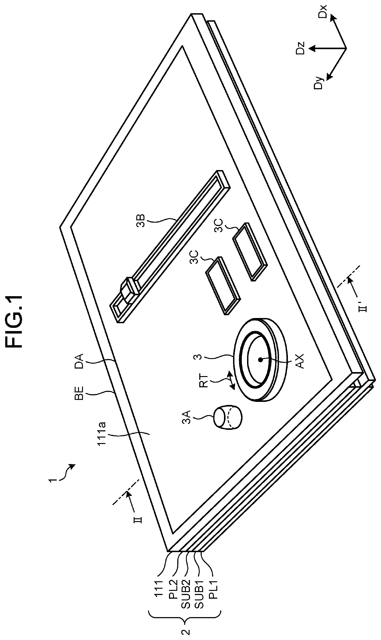
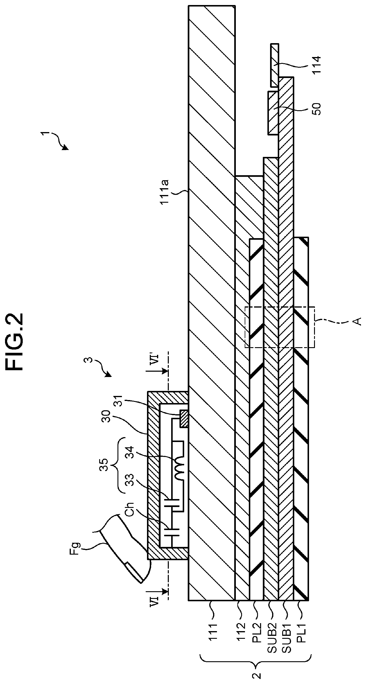
[0034]FIG. 1 is a perspective view schematically illustrating an input detection system according to a first embodiment. FIG. 2 is a cross-sectional view cut along line II-II′ in FIG. 1. As illustrated in FIG. 1 and FIG. 2, an input detection system 1 includes a display device 2 and an input support device (input device) 3.
[0035]One direction of a plane (upper surface 111a) of the display device 2 is a first direction Dx, and a direction orthogonal to the first direction Dx is a second direction Dy. The second direction Dy is not limited thereto and may intersect with the first direction Dx at an angle other than 90°. A third direction Dz orthogonal to the first direction Dx and the second direction Dy corresponds to the thickness direction of an array substrate SUB1.
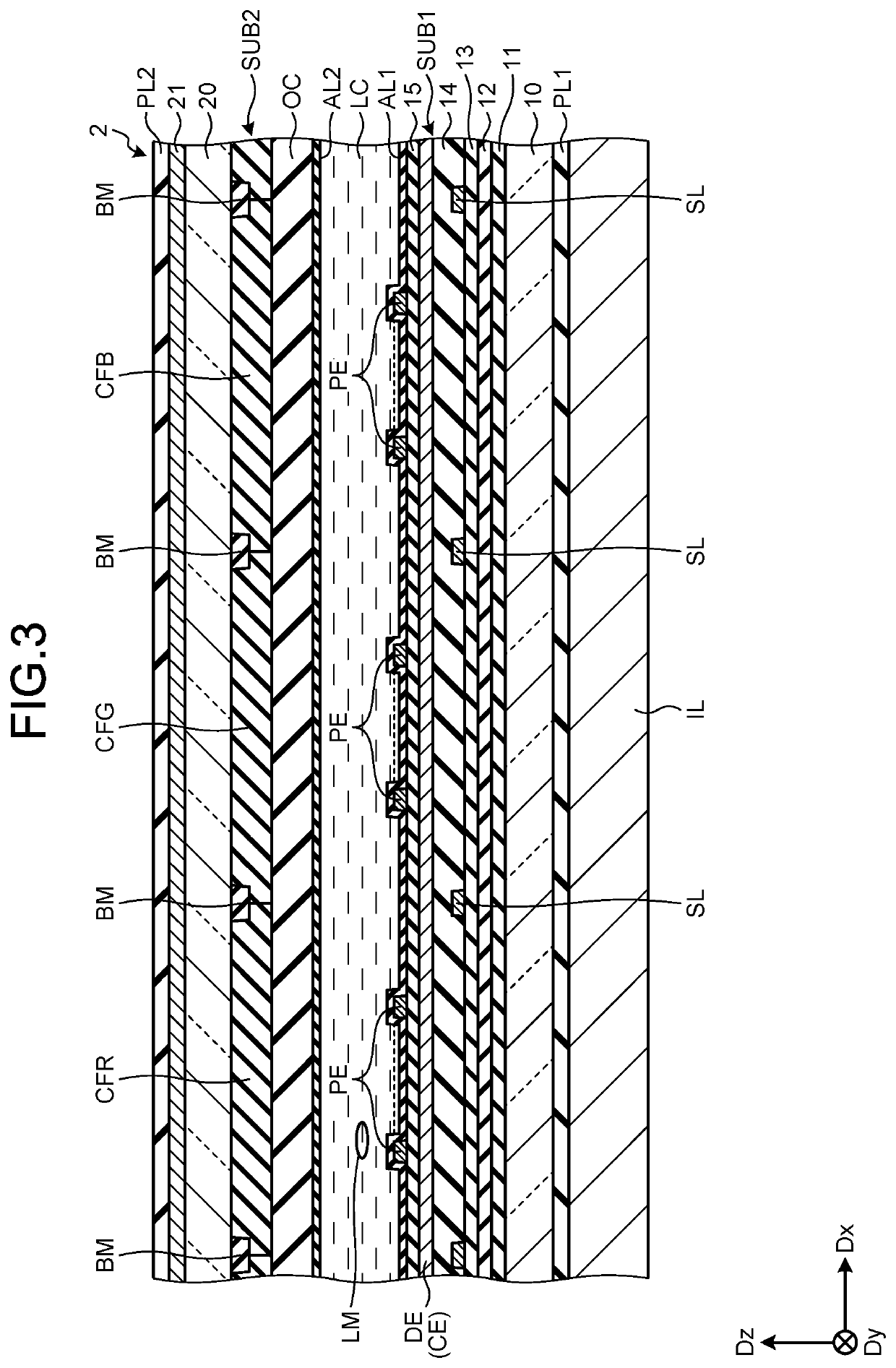
[0036]As illustrated in FIG. 1, the display device 2 includes the array substrate SUB1, a counter substrate SUB2, a first polarizing plate PL1, a second polarizing plate PL2, a cover member 111, and an adhesive layer 11...
first modification
[0097]FIG. 11 is a descriptive view for explaining the configuration of an input support device in a first modification. In the following explanation, the same reference numerals denote the same components described in the above-mentioned embodiment and overlapped explanation thereof is omitted.
[0098]As illustrated in FIG. 11, an input detection system 1a in the first modification is different from that in the above-mentioned first embodiment in the configuration in which an input support device 3a includes no capacitor Ch. That is to say, the coupling portion N1 of the LC circuit 35 on the one end side is coupled to the housing 30 not through the capacitor Ch but through a coupling member 37. The coupling member 37 is, for example wiring formed by a conductor. Any shape and configuration of the coupling member 37 may be employed as long as the coupling member 37 can electrically couple the coupling portion N1 and the housing 30.
[0099]In the first modification, the input support dev...
second modification
[0100]FIG. 12 is a descriptive view for explaining the configuration of an input support device in a second modification. As illustrated in FIG. 12, an input detection system 1b in the second modification is different from that in the above-mentioned first embodiment in the configuration in which the housing 30 of an input support device 3b includes a first housing 30a and a second housing 30b.
[0101]The first housing 30a is formed by a conductor and is located in an upper portion of the housing 30. The first housing 30a is formed to have a projecting shape and has an opening formed on the array substrate SUB1 side. The coupling portion N1 of the LC circuit 35 on the one end side is coupled to the first housing 30a through the capacitor Ch.
[0102]The second housing 30b is formed by a non-conductor made of a resin material, for example, and is located in a lower portion of the housing 30. The second housing 30b is coupled to the first housing 30a and is located between the detection e...
PUM
 Abstract
Description
Claims
Application Information
 - R&D Engineer
- R&D Manager
- IP Professional
- Industry Leading Data Capabilities
- Powerful AI technology
- Patent DNA Extraction
Browse by: Latest US Patents, China's latest patents, Technical Efficacy Thesaurus, Application Domain, Technology Topic.
© 2024 PatSnap. All rights reserved.Legal|Privacy policy|Modern Slavery Act Transparency Statement|Sitemap