Device for re-directing light from optical waveguide

a technology of optical waveguides and devices, applied in the direction of instruments, semiconductor lasers, optical elements, etc., can solve the problems of difficult to manufacture accurately and inexpensively, many of the known arrangements,

Inactive Publication Date: 2000-08-22
KOTURA
View PDF15 Cites 80 Cited by
  • Summary
  • Abstract
  • Description
  • Claims
  • Application Information

AI Technical Summary

Problems solved by technology

Many of the known arrangements are however, difficult to fabricate accurately and inexpensively due to the requirement of ensuring accurate positioning and alignment of the various components concerned.

Method used


Image

  • Device for re-directing light from optical waveguide
  • Device for re-directing light from optical waveguide
  • Device for re-directing light from optical waveguide

Examples


Embodiment Construction

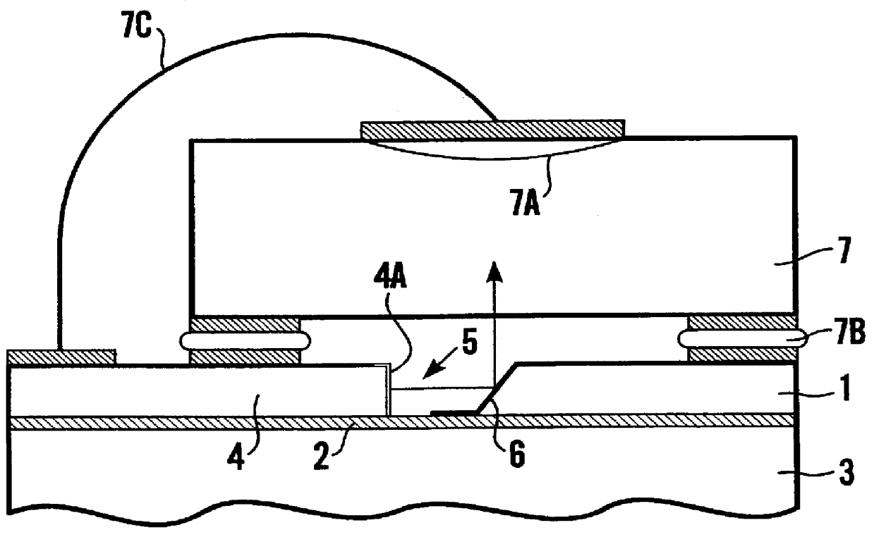
As indicated above, this invention relates to devices formed on silicon-on-insulator wafers which are readily commercially available. The chip comprises a layer of silicon separated from a silicon substrate by a layer of silicon dioxide. The thickness of the upper layer of silicon is typically increased to the required size by epitaxial growth.

Integrated optical waveguides in the form of ribs may be formed in the upper silicon layer. Methods of manufacturing such waveguides are described in the paper "Low loss single mode optical waveguides with large cross-section in silicon-on-insulator" by J. Schmidtchen et al, Electronic Letters, 27, p1486, 1991.

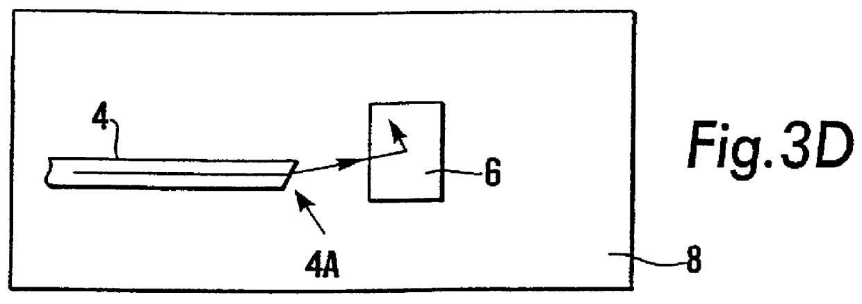
FIG. 2 shows the silicon layer 1, the silicon dioxide layer 2 and the silicon substrate 3. A rib waveguide 4 is formed in the silicon layer 1 which is typically around 5 or 10 microns in thickness. The waveguide 4 terminates at a facet 4A in a recess 5 formed in the silicon layer 1. On the opposite side of the recess 5 a facet 6 is forme...


PUM


Abstract

The device is formed on a silicon-on-insulator chip (which comprises a layer of silicon (1) separated from a substrate (3) by an insulator layer (2)) and comprises an integrated waveguide (4) formed in the silicon layer (1) and a reflective facet (6) formed in a recess in the silicon layer (1). The facet (6) is positioned to redirect light in a desired direction. The waveguide (4) and facet (6) are both formed in the silicon layer (1) so their positions can be defined by the same lithographic steps so they are automatically aligned with each other.

Description

This invention relates to a device for re-directing light from an optical waveguide on a silicon-on-insulator chip.In integrated optical circuits, there is often a requirement to re-direct light from an optical waveguide, e.g. from a waveguide formed on the chip to a receiver such as a photodiode, mounted on the chip. A variety of ways of achieving this have been proposed in a variety of types of integrated optical circuits, e.g. by positioning a photodiode within a recess formed in the chip so it receives light emerging from a waveguide on the chip. Many of the known arrangements are however, difficult to fabricate accurately and inexpensively due to the requirement of ensuring accurate positioning and alignment of the various components concerned.This invention aims to provide a device formed on a silicon-on-insulator chip and which employs features of such a chip and of waveguides formed thereon to assist in the alignment of the components of the device.DISCLOSURE OF INVENTIONAcc...

Claims


Application Information

Patent Timeline
Patent Type & Authority Patents(United States)
IPC IPC(8): G02B6/42H01L31/0232H01S5/02H01S5/00
CPCG02B6/4214H01L31/0232H01S5/02H01L31/02325
Inventor RICKMAN, ANDREW GEORGEHARPIN, ARNOLD PETER ROSCOEMORRIS, ROBIN JEREMY RICHARDGORTON, STEPHENASGHARI, MEHDI
Owner KOTURA
Why Eureka
Try Eureka