Silicon quantum wires

a technology of quantum wires and silicon, applied in the direction of electrical apparatus, nanotechnology, semiconductor devices, etc., can solve the problems of insufficient prior art of furukawa et al, poor luminescence properties of undoped silicon, and the inability to significantly improve the effect of undoped silicon

Inactive Publication Date: 2002-04-09
CHEMTRON RES
View PDF23 Cites 19 Cited by
  • Summary
  • Abstract
  • Description
  • Claims
  • Application Information

AI Technical Summary

Benefits of technology

The invention provides the advantage that it is a simple but effective technique of producing silicon quantum wires particularly silicon quantum wires with diameters of 3 nm or less. Material processed in accordance with the invention has exhibited photoluminescence similar to that of Furukawa et al for quantum dots. This indicates that wire diameters in the region of 3 nm or less have been achieved.
Anodization may be carried out to produce porosity in the range 20% to 80%, and etching may then be performed at a rate in the range 0.0001 nm to 10 nm per minute to provide an increase in porosity to a value in the range 60% to 90%. The etch rate is preferably in the range 0.01 nm to 10 nm per minute. To minimise processing costs, the etch rate should be as high as possible consistent with the production of well-defined quantum wires. Anodization may be carried out in aqueous or ethanoic hydrofluoric acid of concentration in the range 10% to 50% by weight. An anodizing current density of 5 to 500 mAmp / cm.sup.2 may be applied for 10 to 6000 seconds, as appropriate to requirements of layer thickness, porosity and conductivity magnitude and type.

Problems solved by technology

Bulk undoped silicon is unfortunately characterised by very poor luminescent properties.
In this regard, the prior art of Furukawa et al is inappropriate.
It seems unlikely that this can be significantly improved due to the difficulty of obtaining conduction between adjacent crystallites.

Method used


Image

  • Silicon quantum wires
  • Silicon quantum wires
  • Silicon quantum wires

Examples


Embodiment Construction

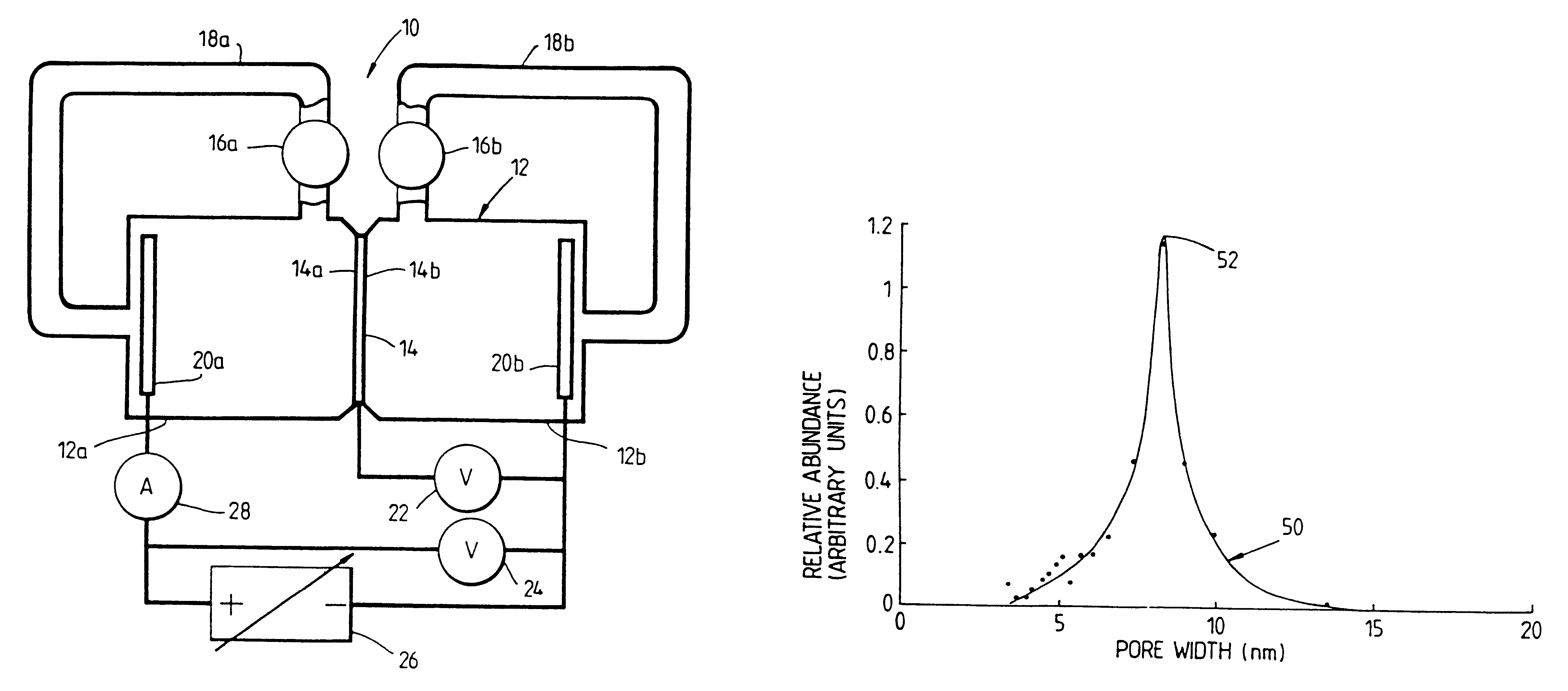
Referring to FIG. 1, an electrochemical apparatus 10 for processing semiconductor material in accordance with the invention is shown schematically. The apparatus 10 incorporates an electrochemical cell 12 divided into left and right halt cells 12a and 12b by a silicon wafer 14 to be processed. The half cells 12a and 12b are connected to dual purpose pumps 16a and 16b by pipes 18a and 18b respectively. Each combination of elements 12a / 16a / 18a and 12b / 16b / 18b forms a closed loop for electrolyte recirculation. The half cells 12a and 12b incorporate respective platinum electrodes 20a (anode) and 20b (cathode). A first voltmeter 22 is connected between the Si wafer 14 and the cathode 20b, and a second voltmeter 24 is connected between the anode 20a and the cathode 20b. A galvanostat 26, ie a constant current source, is connected in series with an ammeter 28, and this series arrangement is connected between the anode 20a and the cathode 20b.

The apparatus 10 is hinged (not shown) in the re...


PUM


Abstract

A method of making semiconductor quantum wires employs a semiconductor wafer (14) as starting material. The wafer (14) is weakly doped p type with a shallow heavily doped p layer therein for current flow uniformity purposes. The wafer (14) is anodised in 20% aqueous hydrofluoric acid to produce a layer (5) microns thick with 70% porosity and good crystallinity. The layer is subsequently etched in concentrated hydrofluoric acid, which provides a slow etch rate. The etch increases porosity to a level in the region of 80% or above. At such a level, pores overlap and isolated quantum wires are expected to form with diameters less than or equal to 3 nm. The etched layer exhibits photoluminescence emission at photon energies well above the silicon bandgap (1.1 eV) and extending into the red region (1.6-2.0 eV) of the visible spectrum.

Description

1. Field of the InventionThis invention relates to a method of making silicon quantum wires and to devices made by the method.2. Discussion of Prior ArtSemiconductor quantum wires are a recent development in the emerging field of low dimensional semiconductor device structures. The first such structure was the one dimensional quantum well, in which a relatively narrow bandgap semiconductor layer is sandwiched between two relatively wider bandgap semiconductor layers. A typical quantum well layer thickness is in the range 1 to 10 nm. Charge carriers with energies intermediate the bandgaps of the two materials are free in the narrow bandgap material but would be bound in the wider bandgap material. This produces what is referred to as quantum confinement of charge carriers within a quantum well formed by a narrow bandgap layer. There is two-dimensional freedom for charge carriers within the plane of the layer, and one-dimensional confinement. This provides a quantum well layer or "qua...

Claims


Application Information

Patent Timeline
Patent Type & Authority Patents(United States)
IPC IPC(8): H01L21/306H01L21/02H01L29/06H01L33/34
CPCB82Y10/00H01L21/306H01L33/346Y10S438/96Y10S438/962
Inventor CANHAM, LEIGH-TREVORKEEN, JOHN MICHAELLEONG, WENG YEE
Owner CHEMTRON RES
Why Eureka
Try Eureka