Direct access logic testing in integrated circuits

Inactive Publication Date: 2002-05-07
RENESAS ELECTRONICS AMERICA
View PDF9 Cites 14 Cited by
  • Summary
  • Abstract
  • Description
  • Claims
  • Application Information

AI Technical Summary

Benefits of technology

FIG. 5 shown is a related-art environment wherein the embodiment of the invention set forth in FIG. 3 proves particularly useful.

Problems solved by technology

However, as noted, the design process rarely proceeds at a lower level than that of logic diagrams.
The regions affected by the selective manipulation of the single piece of semiconductor material are almost unimaginably small.
Furthermore, the sizes of the regions manipulated decrease virtually every week.
Due to the very small regions manipulated during VLSI production, errors invariably occur.
This can be the result of contamination of the material, or minor variations in the length, width, or height of lines etched.
These errors in production often result in errors in the behavior of the discrete electronic circuit level components.
Consequently, errors in production sufficient to produce errors in the behavior of the discrete circuit level components can "propagate" upwards to the logic diagram level since the logic diagram circuits are built from congeries of these malfunctioning circuit components.
If the errors are severe, then such malfunctioning will be very apparent in that the affected logic diagram level circuits will not function.
However, if the malfunction is not severe, it is possible that the affected logic diagram level components will perform, but will perform in such a way that is out of design tolerances, which can cause a

Method used


Image

  • Direct access logic testing in integrated circuits
  • Direct access logic testing in integrated circuits
  • Direct access logic testing in integrated circuits

Examples


Embodiment Construction

)

The following sets forth a detailed description of the best contemplated mode for carrying out the invention as described in the claims. The detailed description is intended to be illustrative and should not be taken as limiting.

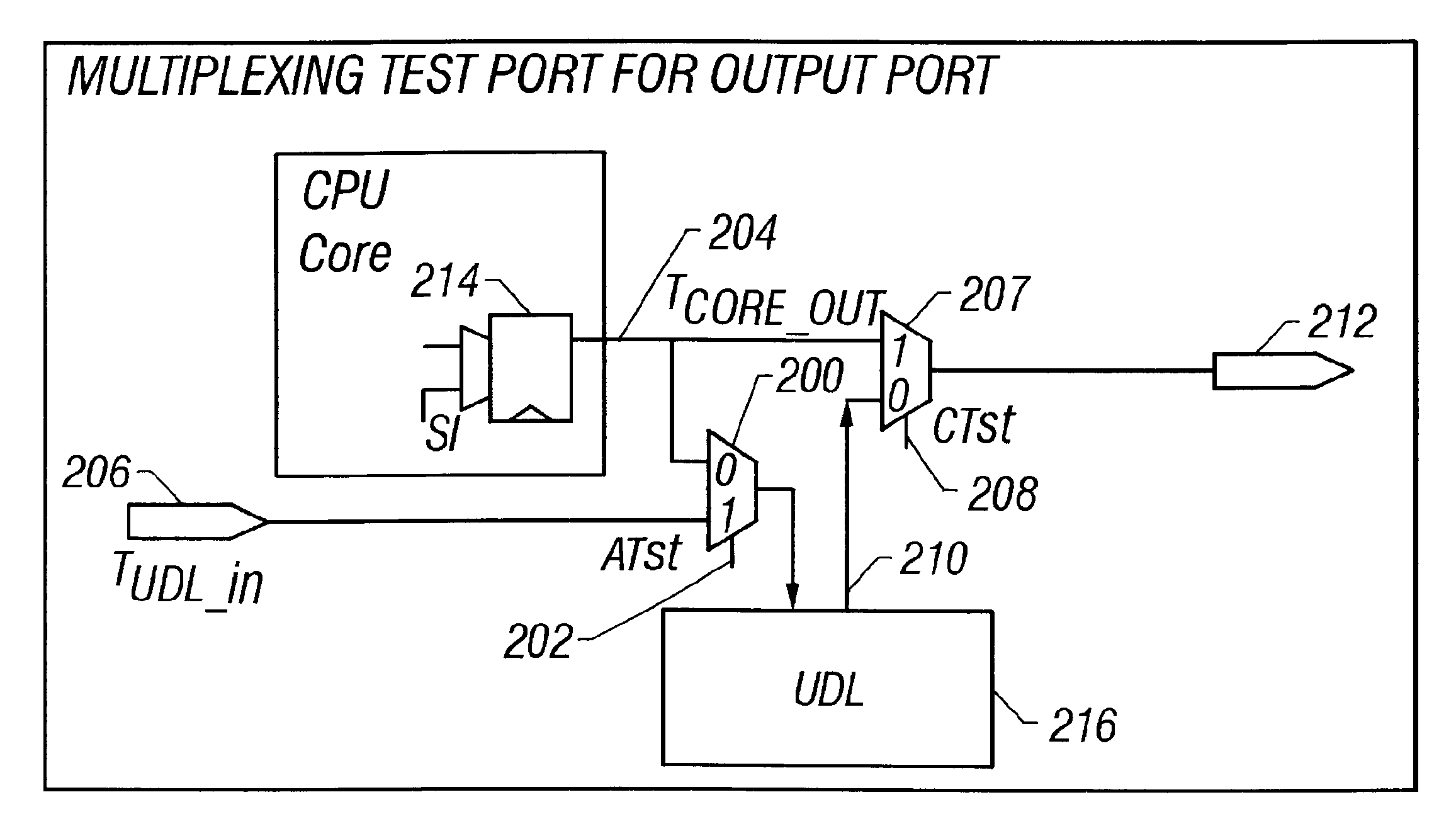
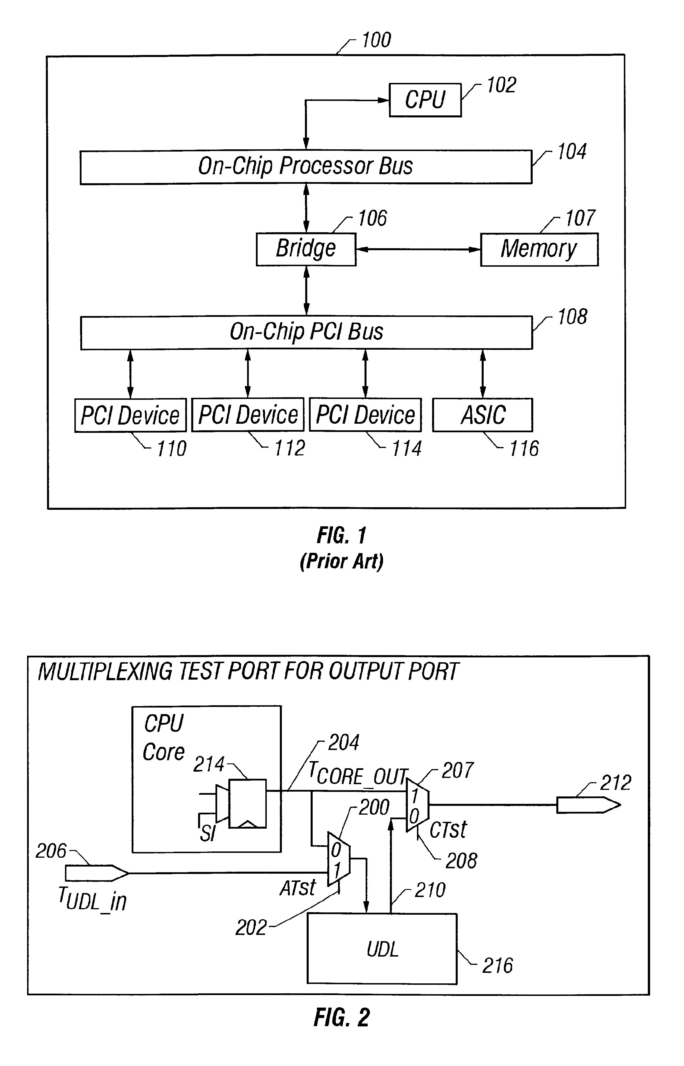
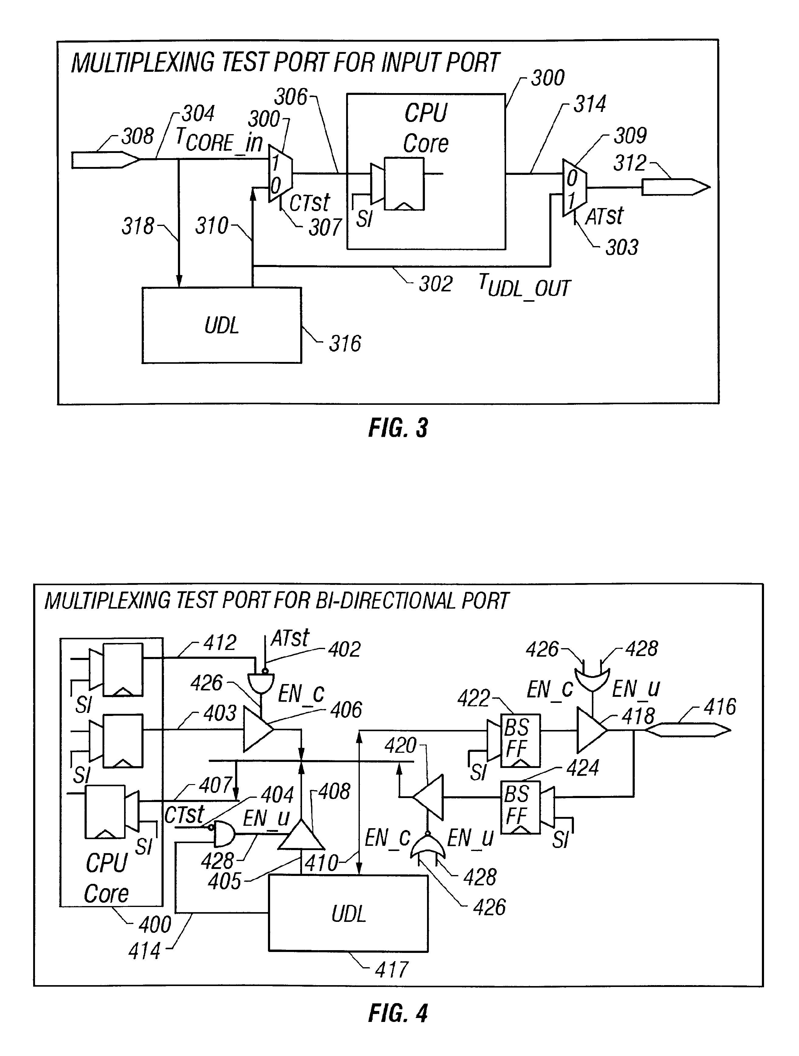
In various embodiments of the present invention, the various cores and UDL are fully verified (i.e., accessed and tested) independent of each other. The various embodiments of the present invention provide several modes of operation, examples of which are illustrated in FIGS. 2, 3, and 4 in conjunction with Table 1. Table 1 illustrates that in certain exemplary embodiments, the control of the exemplary modes is achieved by two test control signals, ATst and CTst.

Certain embodiments of the present invention support the three operation modes illustrated within Table 1 by providing an I / O interface between at least one core and at least one UDL which allows usage of the mode select signals (i.e. ATst or CTst) illustrated in Table 1. The embodiments set forth b...


PUM


Abstract

A method and circuit for allowing direct access logic testing in integrated circuits. In one embodiment, an interface between integrated circuit core logic and integrated circuit user-defined logic is exposed, and the integrated circuit core logic and the integrated circuit user-defined logic is tested via the exposed interface. In another embodiment, an integrated circuit has logic selection circuitry connected with core logic and user-defined logic. The logic selection circuitry is used to selectively test the core logic and user-defined logic.

Description

1. Field of the InventionThis invention relates to the field of integrated circuit testing.2. Description of the Related ArtAn integrated circuit (IC) is a miniature electric circuit containing large numbers of discrete electronic circuit elements, such as transistors, resistors, capacitors, and diodes, which are packaged as a single unit with leads extending from it for input, output, and power-supply connections. The electronic circuit elements are formed by selective manipulation of a single chip of semiconductor material, often in combination with various other semi-conducting and / or conducting materials.It is common in the art to roughly classify integrated circuits dependent upon their transistor density. Presently, there are effectively four common integrated circuit classifications: small-scale integrated circuits (SSIs); medium-scale integrated circuits (MSIs); large-scale integrated circuits (LSIs); and very-large-scale integrated circuit (VLSIs). Exactly what transistor d...

Claims


Application Information

Patent Timeline
IPC IPC(8): G01R31/317G01R31/28G01R31/3185
CPCG01R31/318516G01R31/31701
Inventor CHEN, PINGKOE, WERN-YAN
Owner RENESAS ELECTRONICS AMERICA
Why Eureka
Try Eureka