Cup shaped plating apparatus with a disc shaped stirring device having an opening in the center thereof

a technology of stirring device and cup-shaped plating, which is applied in the direction of electrolysis components, manufacturing tools, cell components, etc., can solve the problems of unsatisfactory industrial production yield, unsatisfactory yield of industrial production, and uniform plating on annular edge portion of wafer surface to be plated

Inactive Publication Date: 2002-11-19
ELECTROPLATING ENGINEERS OF JAPAN LTD
View PDF4 Cites 21 Cited by
  • Summary
  • Abstract
  • Description
  • Claims
  • Application Information

AI Technical Summary

Benefits of technology

In the conventional cup-type plating apparatus described in the above, since the plating solution supplied into the plating tank by virtue of its upward flow is caused to spread radially and constantly from an area near the center of the surface to be plated to the annular edge portion thereof, the concentration of metallic ions of the plating solution near the annular edge portion of the surface to be plated is likely to be different from that near the center of the same surface to be plated. Particularly, when an electric current density is increased, the nature of the plating treatment near the center of the surface to be plated will be different from that near the annular edge portion of the same surface to be plated, resulting in an ununiform plating treatment. In contrast, with the use of the cup-type plating apparatus of the present invention, an upward flow of the plating solution supplied through the at least one plating-solution-supply pipe will be changed in its flowing direction by virtue of the stirring device. Consequently, if viewed on the entire surface to be plated, the plating solution will be in a relatively random flowing state so as to get full contact with the surface to be plated of a wafer. Therefore, the metallic ions of the plating solution are allowed to be uniformly supplied to the entire surface to be plated of a wafer, thus effecting a plating treatment having an extremely high uniformity. Further, since the plating solution is in a relatively random flowing state when getting in contact with the surface to be plated, it is possible to avoid the occurrence of an ununiformly plated external appearance which would otherwise be caused due to an ununiform spreading of the plating solution.
In this way, the plating solution supplied to the plating tank by virtue of its upward flow is allowed to pass through the center opening of the doughnut-like disc so as to arrive at the surface to be plated of a wafer. Then, the flowing state of the plating solution spreading radially towards the annular edge portion of the surface to be plated of a wafer will be changed by the stirring blade. Therefore, it is possible to eliminate the flow retardation of the plating solution which would otherwise be caused due to a slight height difference between the plating-solution-outlet passages (provided below the wafer support section) on one hand and the surface to be plated of the wafer (mounted on the wafer support section) on the other, thereby making it possible to perform a uniform plating treatment on the entire surface to be plated including its annular edge portion.

Problems solved by technology

However, in the conventional cup-type plating apparatus described in the above, since there is a small height difference between the plating-solution-outlet passages (provided under the wafer support section) on one hand and the surface to be plated of a wafer (mounted on the wafer support section) on the other, an undesired corner area is formed therebetween.
As a result, a flow retardation of the plating solution will occur in the corner area, thus causing an ununiform plating on an annular edge portion of the wafer surface to be plated.
Consequently, a semiconductor wafer treated in this way is greatly limited in its effectively usable area, resulting in an unsatisfactory yield in industrial production.
However, in using the above described conventional cup-type plating apparatus, since the flowing state of the plating solution on the surface to be plated of a wafer is so formed that the plating solution will spread radially and constantly from an area near the center of the surface to be plated to the annular edge portion thereof, it is difficult to effect a uniform plating treatment on the entire surface to be plated having a fine wiring pattern formed thereon.
Further, since it has been difficult to cover the entire wafer surface to be plated including its annular edge portion with plating solution, it has been also difficult to ensure a uniform plating treatment on a large area of a wafer.
Particularly, when an electric current density is increased, the nature of the plating treatment near the center of the surface to be plated will be different from that near the annular edge portion of the same surface to be plated, resulting in an ununiform plating treatment.

Method used


Image

  • Cup shaped plating apparatus with a disc shaped stirring device having an opening in the center thereof
  • Cup shaped plating apparatus with a disc shaped stirring device having an opening in the center thereof
  • Cup shaped plating apparatus with a disc shaped stirring device having an opening in the center thereof

Examples


Embodiment Construction

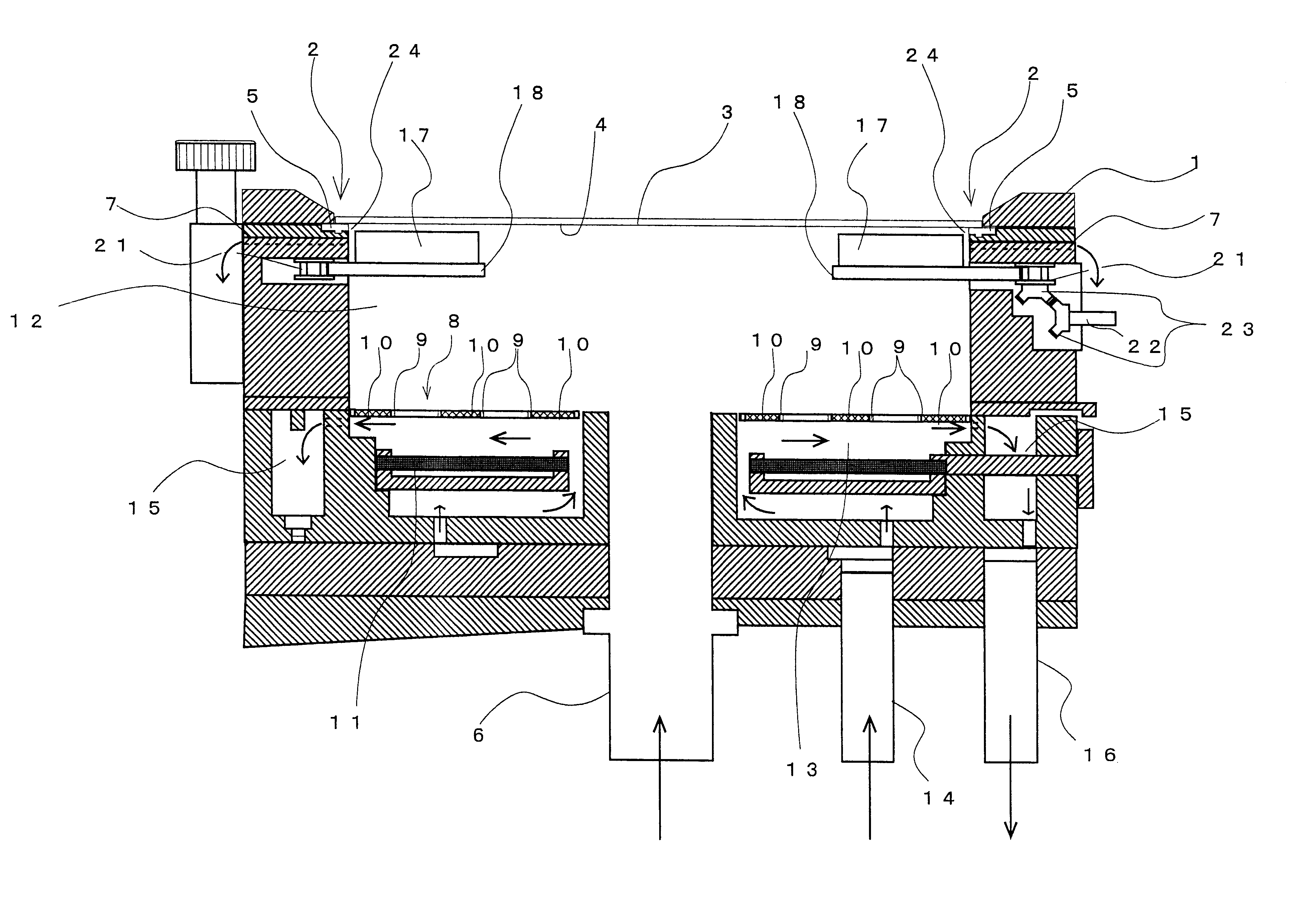
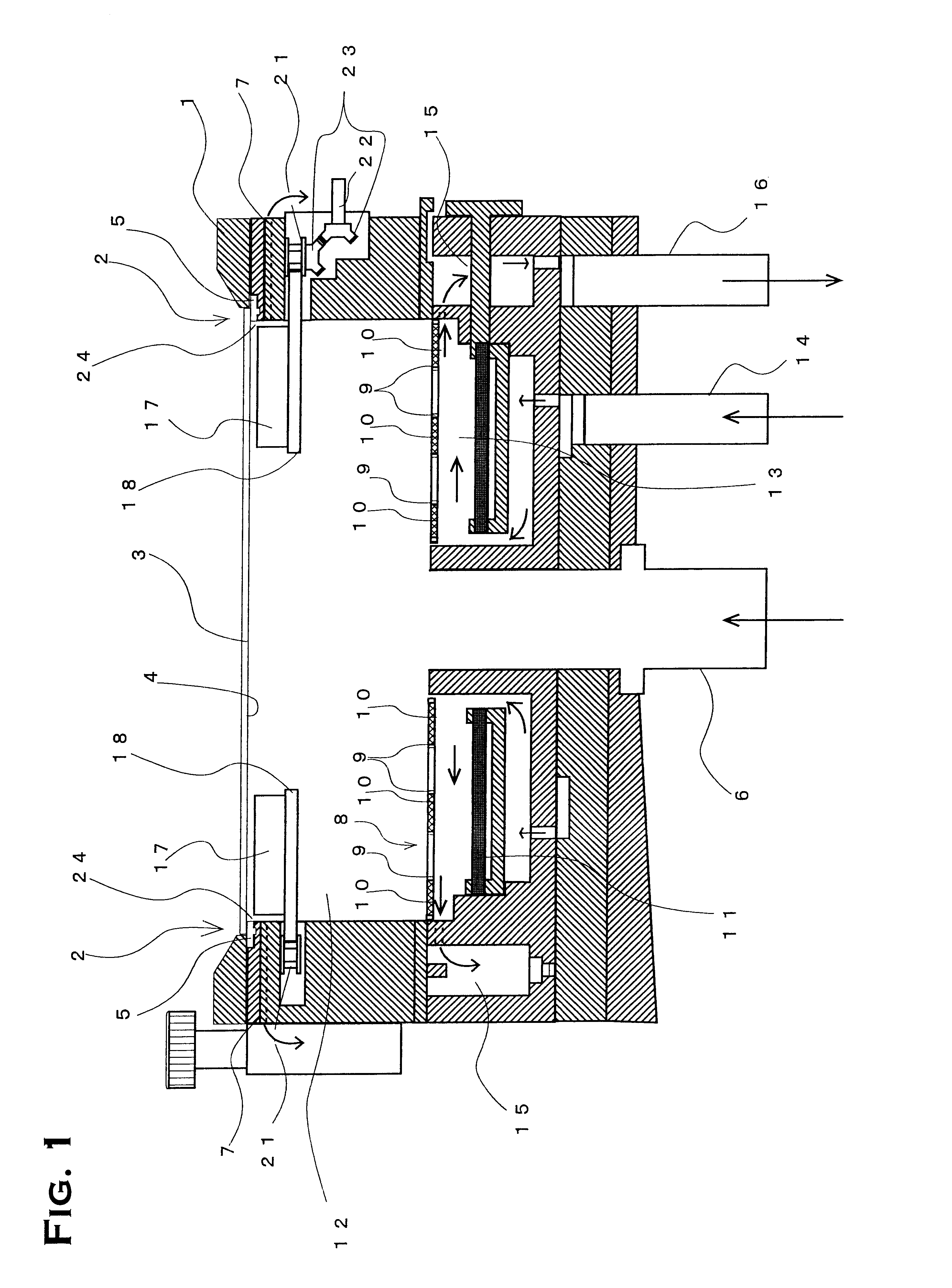
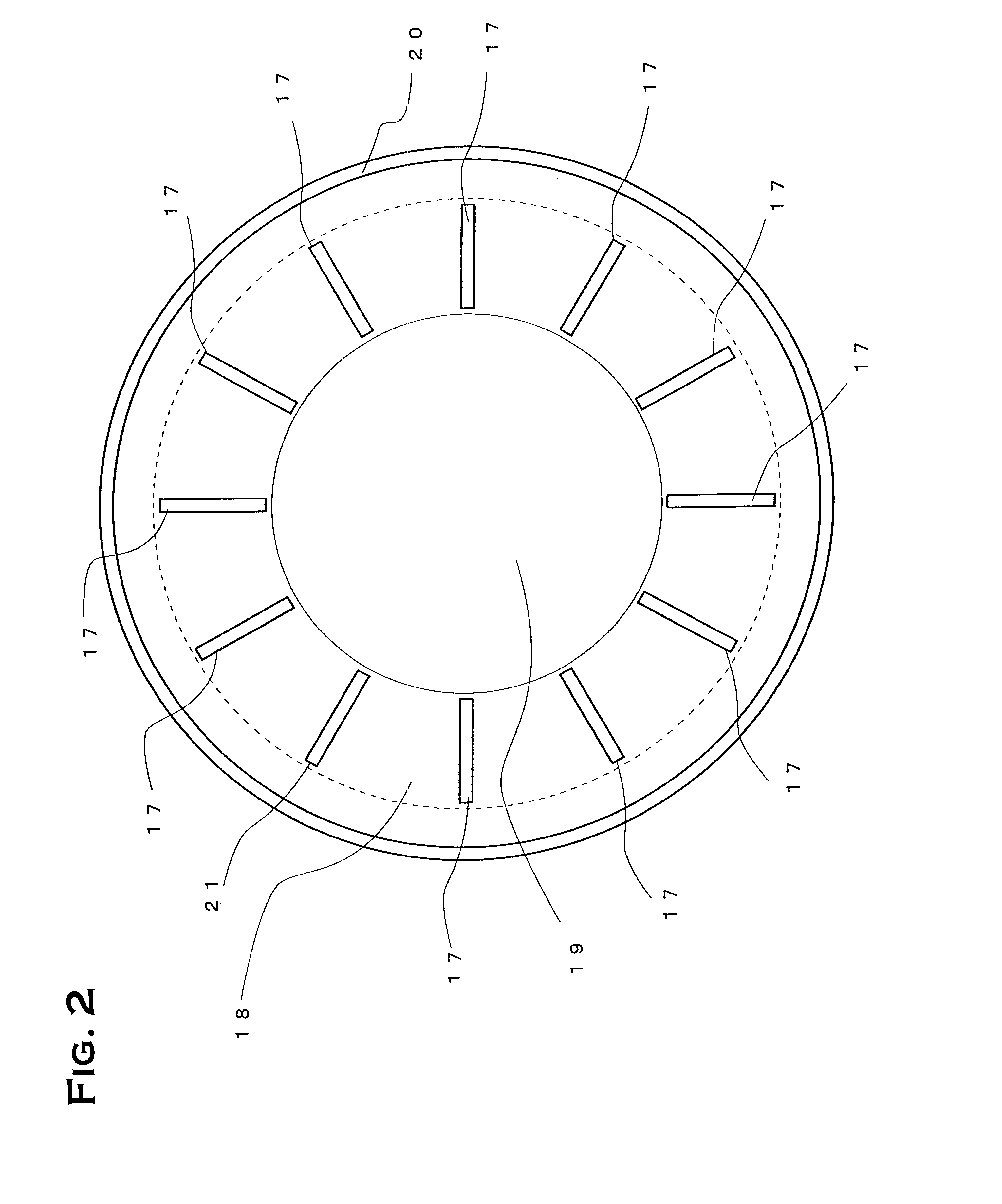
In the following, description will be given to explain in detail a preferred embodiment of a cup-type plating apparatus formed according to the present invention. FIG. 1 is a sectional view schematically showing the cup-type plating apparatus of the present embodiment. As shown in FIG. 1, the cup-type plating apparatus of this embodiment comprises a wafer support section 2 provided along an upper opening of a plating tank 1. A wafer 3 is mounted on the wafer support section 2. In this way, a plating treatment is performed on a surface 4 to be plated of the wafer 3. The wafer support section 2 comprises a not-shown cathode and a seal packing 5 provided beneath the cathode for preventing a possible leakage of the plating solution.

Further, on the central bottom of the plating tank 1 there is provided a main-plating-solution supply pipe 6. Below the wafer support section 2 there are provided a plurality of solution-outlet passages 7 which are used to cause the plating solution arriving ...


PUM

PropertyMeasurementUnit
heightaaaaaaaaaa
areaaaaaaaaaaa
concentrationaaaaaaaaaa

Abstract

This invention provides a technique capable of solving a problem of an ununiform plating on an annular edge portion of a surface to be plated of a wafer, which ununiform plating is usually caused due to an ununiform flow of a plating apparatus, thereby ensuring a uniform plating treatment on the entire surface to be plated of a wafer. The present invention is directed to a cup-shaped plating apparatus comprising a wafer support section provided along an upper opening of a plating tank, a plurality of solution-outlet passages provided below the wafer support section and extending from the inside of and to the outside of the plating tank and at least one solution-supply pipe provided through the bottom of the plating tank.

Description

1. Technical Field of the InventionThe present invention relates to a cup-type plating apparatus for carrying out a plating treatment on a semiconductor wafer.2. Description of the Related ArtConventionally, there has been known and in practical use a cup-type plating apparatus for carrying out a plating treatment on a semiconductor wafer. Such a cup-type plating apparatus comprises a wafer support section provided along an upper opening of a plating tank, a plurality of plating-solution-outlet passages provided below the wafer support section and extending from the inside of the plating tank to the outside thereof, at least one plating-solution-supply pipe provided through the bottom of the plating tank. In detail, a plating solution supplied to the plating tank through the at least one plating-solution-supply pipe by virtue of an upward flow of the plating solution, is caused to form a plurality of outward flows passing through the plurality of plating-solution-outlet passages and...

Claims


Application Information

Patent Timeline
Patent Type & Authority Patents(United States)
IPC IPC(8): C25D7/12H01L21/02H01L21/288
CPCH01L21/2885C25D17/001Y10S204/07
Inventor SAKAKI, YASUHIKO
Owner ELECTROPLATING ENGINEERS OF JAPAN LTD
Why Eureka
Try Eureka