Tape having implantable conductive lands for semiconductor packaging process and method for manufacturing the same

a technology of conductive lands and semiconductor packaging, which is applied in the direction of semiconductor devices, semiconductor/solid-state device details, electrical apparatus, etc., can solve the problems of reducing the electrical performance of a bga package, encapsulating and attaching external connecting terminals, and minimizing the thickness of the semiconductor packag

Inactive Publication Date: 2003-01-14
KOSTAT SEMICON
View PDF8 Cites 161 Cited by
  • Summary
  • Abstract
  • Description
  • Claims
  • Application Information

AI Technical Summary

Problems solved by technology

Such a rigid substrate remains within a semiconductor package as a part thereof after completion of assembly of the semiconductor package, so it is an obstacle in minimizing the thickness of the semiconductor package.
However, this case has many difficulties in performing wire bonding, encapsulation and attachment of external connecting terminals.
Firstly, intermediate connectors such as the circuit patterns 12 and 20 formed on the top and bottom of the rigid substrate 10 and via-holes 16 provided between the chip 2 and the external connecting terminals 22 degrade the electrical performance of a BGA package.
Secondarily, the insulation substrate 18 constituting the rigid substrate 10 remains within a BGA package after the completion of assembly of the BGA package, which limits the reduction of the thickness of a semiconductor package. In other words, there is a limitation in reducing the thickness of a semiconductor package.
Thirdly, since a process for forming the solder masks 14 and 14' is required to ensure the insulation between the circuit patterns 12, the manufacturing is complicated.
Finally, the rigid substrate 10 is very elaborate, so it is very difficult to manufacture it and its price is very high.
Therefore, the cost for assembling a BGA package is high.

Method used


Image

  • Tape having implantable conductive lands for semiconductor packaging process and method for manufacturing the same
  • Tape having implantable conductive lands for semiconductor packaging process and method for manufacturing the same
  • Tape having implantable conductive lands for semiconductor packaging process and method for manufacturing the same

Examples


first embodiment

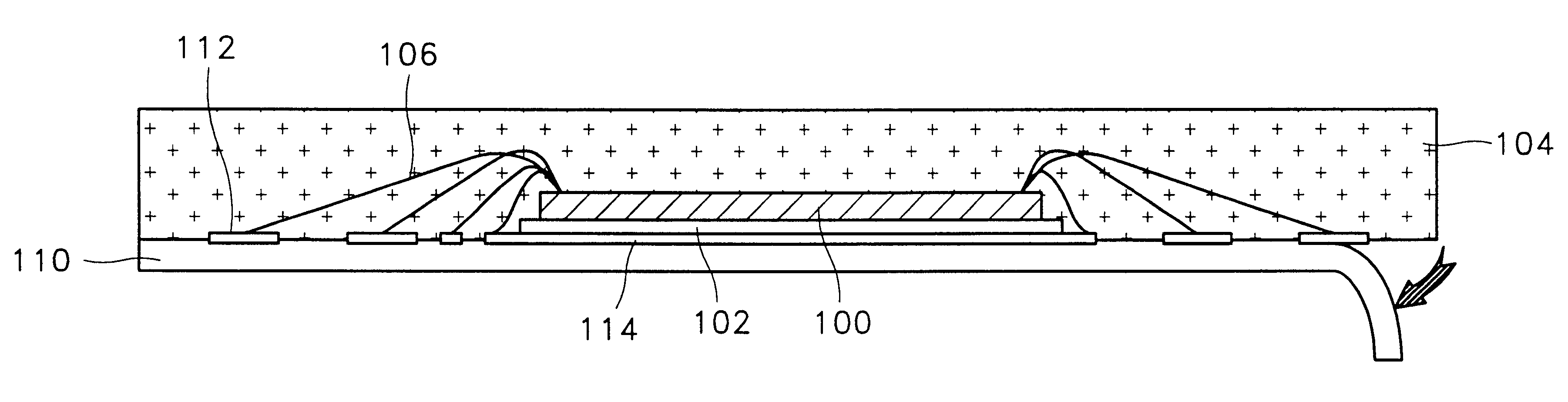
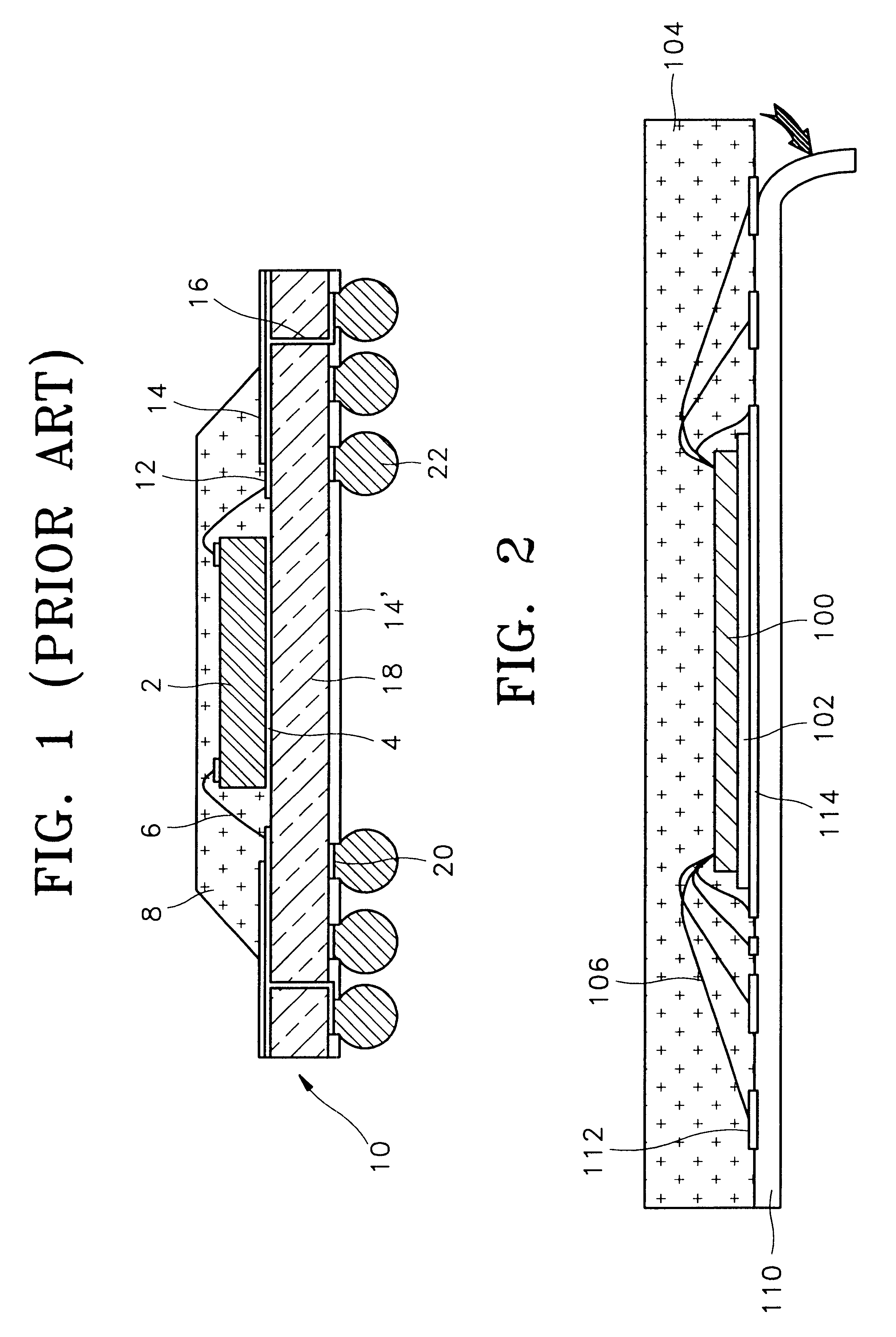
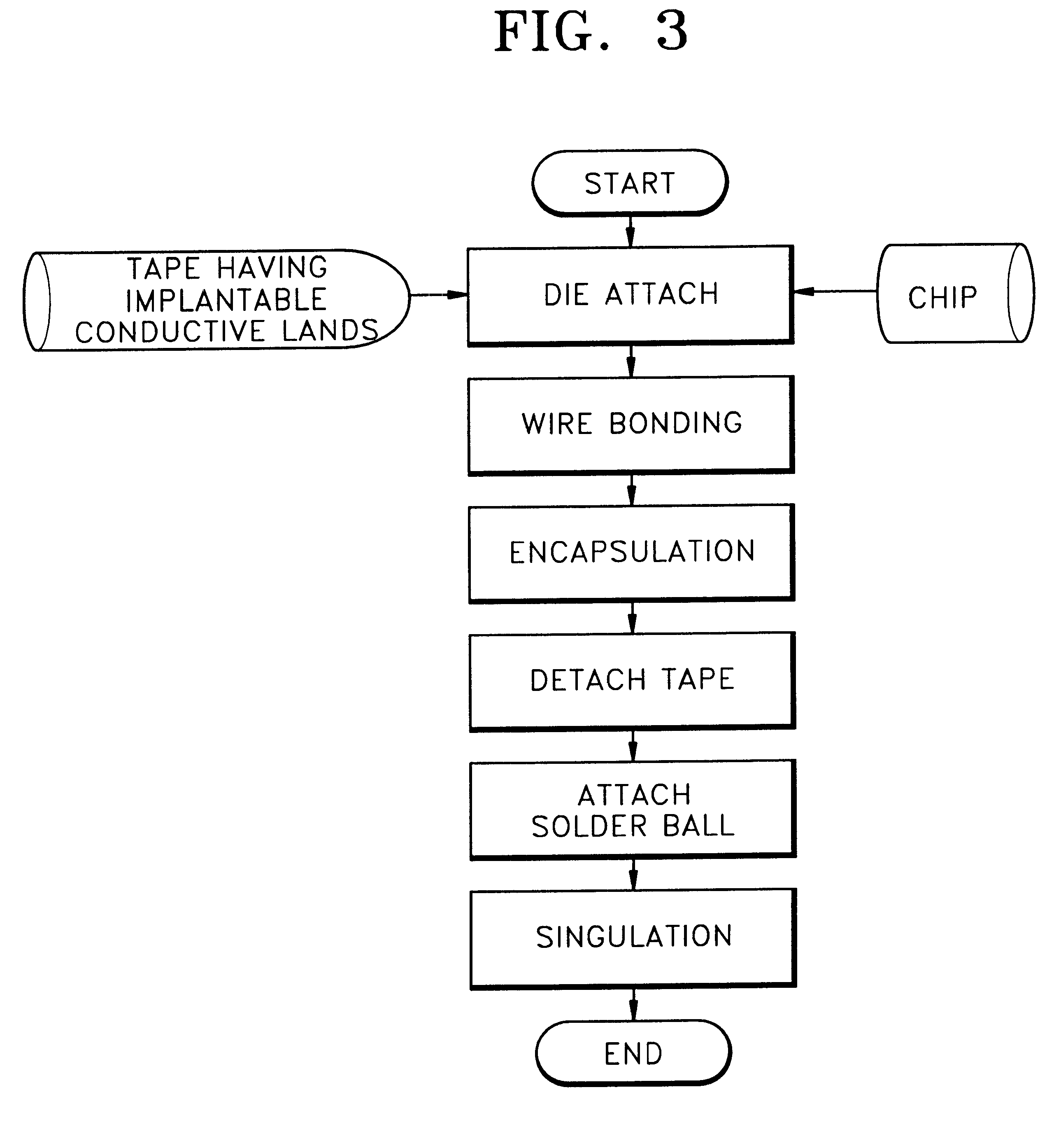
FIG. 9 is a flowchart illustrating a method of manufacturing a tape having implantable conductive lands for a semiconductor packaging process according to a first embodiment of the present invention. Referring to FIG. 9, a tape film including an adhesive layer which can be easily detached from a semiconductor package that is encapsulated with an epoxy mold compound in an encapsulation process is prepared. Next, a copper foil used as an implantable conductive land body is laminated on the tape film. A first photo mask pattern exposing areas for implantable conductive lands is formed on the copper foil. A surface treatment is performed on the exposed areas to form surface treatment layers allowing wire bonding. Subsequently, the first photo mask pattern is removed. Next, a second photo mask pattern exposing the remaining portion other than the areas for implantable conductive lands is formed on the copper foil. An etching process is performed using the second photo mask pattern as an ...

second embodiment

FIG. 10 is a flowchart illustrating a method of manufacturing a tape having implantable conductive lands for a semiconductor packaging process according to a second embodiment of the present invention. Referring to FIG. 10, a tape film including an adhesive layer which can be easily detached from a semiconductor package that is encapsulated with an epoxy mold compound in an encapsulation process is prepared. Next, implantable conductive lands are printed on the tape film with conductive metal paste. A volatile solvent contained in the conductive metal paste is removed by a curing process. Finally, a surface treatment for wire bonding is performed on the printed implantable conductive land.

third embodiment

FIG. 11 is a flowchart illustrating a method of manufacturing a tape having implantable conductive lands for a semiconductor packaging process according to a third embodiment of the present invention. Referring to FIG. 11, a tape film including an adhesive layer which can be easily detached from a semiconductor package that is encapsulated with an epoxy mold compound in an encapsulation process is prepared. Unlike the other embodiments, implantable conductive lands are not formed on the tape film but are formed outside. For example, individual implantable conductive lands are prepared in advance by performing stamping in a press. The implantable conductive lands are then placed on the tape film using a pick and place machine. After completely placing all implantable conductive lands, the tape film and the implantable conductive lands are laminated. After completing the lamination, surface treatment is performed on the second surfaces of the implantable conductive lands. If the secon...


PUM


Abstract

A tape having implantable conductive lands, which realizes a new structure in which an organic rigid substrate is removed from a semiconductor package in a semiconductor packaging process, and a method for manufacturing the tape are provided. The tape includes a tape film, which can be detached from a semiconductor package after an encapsulation process and serves as a general rigid substrate until the encapsulation process is completed, and implantable conductive lands adhering to the tape film. The tape having the implantable conductive lands may be manufactured by laminating a foil for the implantable conductive lands on the tape film and performing photolithography, by printing the implantable conductive lands on the tape film, by attaching the implantable conductive lands that are individually made in advance on the tape film and performing lamination, by depositing and patterning a material layer for the implantable conductive lands on the tape film, or by forming seed layers on the tape film and performing electroplating.

Description

1. Field of the InventionThe present invention relates to assembly of a semiconductor package, and more particularly, to a tape having implantable conductive lands which is substituted for a rigid substrate during processes for manufacturing a semiconductor package such as a ball grid array (BGA) type package, and a method for manufacturing the same.2. Description of the Related ArtRecently, electronic products such as personal computers, cellular phones and camcorders become smaller in size and larger in processing capacity. Accordingly, a semiconductor package which is small in size, large in capacity and compliant with a fast processing speed is fully required. Therefore, semiconductor packages have been transformed from an insertional mounting type including a dual in-line (DIP) package into a surface mounting type including a thin small out-line package (TSOP), a thin quad flat package (TQFP) and a ball grid array (BGA).The BGA, among the surface mounting types, has attracted c...

Claims


Application Information

Patent Timeline
Patent Type & Authority Patents(United States)
IPC IPC(8): H01L21/67H01L21/68H01L21/48H01L21/02H01L23/31H01L23/28H01L23/12H01L21/56
CPCH01L21/4846H01L21/561H01L23/3107H01L21/568H01L2224/32245H01L2224/45144H01L2924/01087H01L24/48H01L2924/15311H01L2924/01079H01L2924/01046H01L2224/73265H01L2224/48247H01L2224/48227H01L2224/48091H01L2224/32225H01L2924/00014H01L2924/00H01L24/45H01L2924/181H01L2924/00012H01L2224/45015H01L2924/207H01L23/28
Inventor GANG, HEUNG-SU
Owner KOSTAT SEMICON
Why Eureka
Try Eureka