Single ended input, differential output amplifier

a technology of differential output and input, applied in the direction of pulse automatic control, pulse manipulation, pulse technique, etc., can solve the problems of bipolar circuits, prohibitively expensive external balun or other tracking filters, and high external tracking filters

Inactive Publication Date: 2003-05-06
NXP USA INC
View PDF5 Cites 26 Cited by
  • Summary
  • Abstract
  • Description
  • Claims
  • Application Information

AI Technical Summary

Problems solved by technology

Traditional wide band amplifiers require very expensive external tracking filters, e.g., an external balun.
For many applications an external balun or other tracking filter is prohibitively expensive and, an on-chip single ended (single phased) input to differential (output) converter is necessary to maintain acceptable linearity and dynamic range.
Prior single ended to differential conversion approaches have resulted in circuits, typically bipolar, with limited dynamic operating range and still some sensitivity to second and third order effects especially at the extremes of that operating range, as well as device noise sensitivity, e.g. from device mismatches.
While second and third order effects could be further reduced, that reduction was at a cost of even further limiting amplifier dynamic operating range.
Further, these single ended to differential bipolar amplifiers do not lend themselves to a field effect transistor (FET) analog.
So, threshold voltages for two matched FETs may exhibit a significant mismatch which reduces linearity.
Thus, even if devices are identical by design, device configuration and bias voltages may be mismatched to cause a transconductance mismatch, severely degrading operation of such an FET amplifier.

Method used


Image

  • Single ended input, differential output amplifier
  • Single ended input, differential output amplifier

Examples


Embodiment Construction

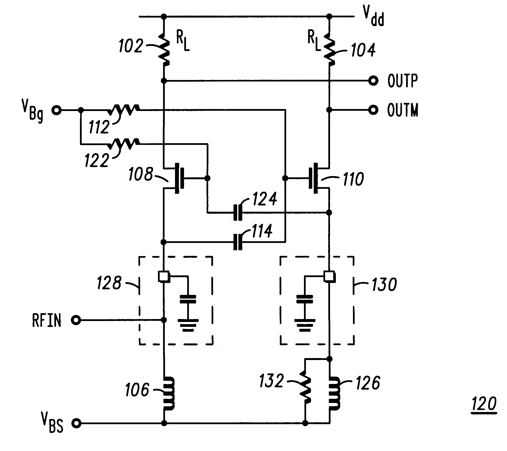
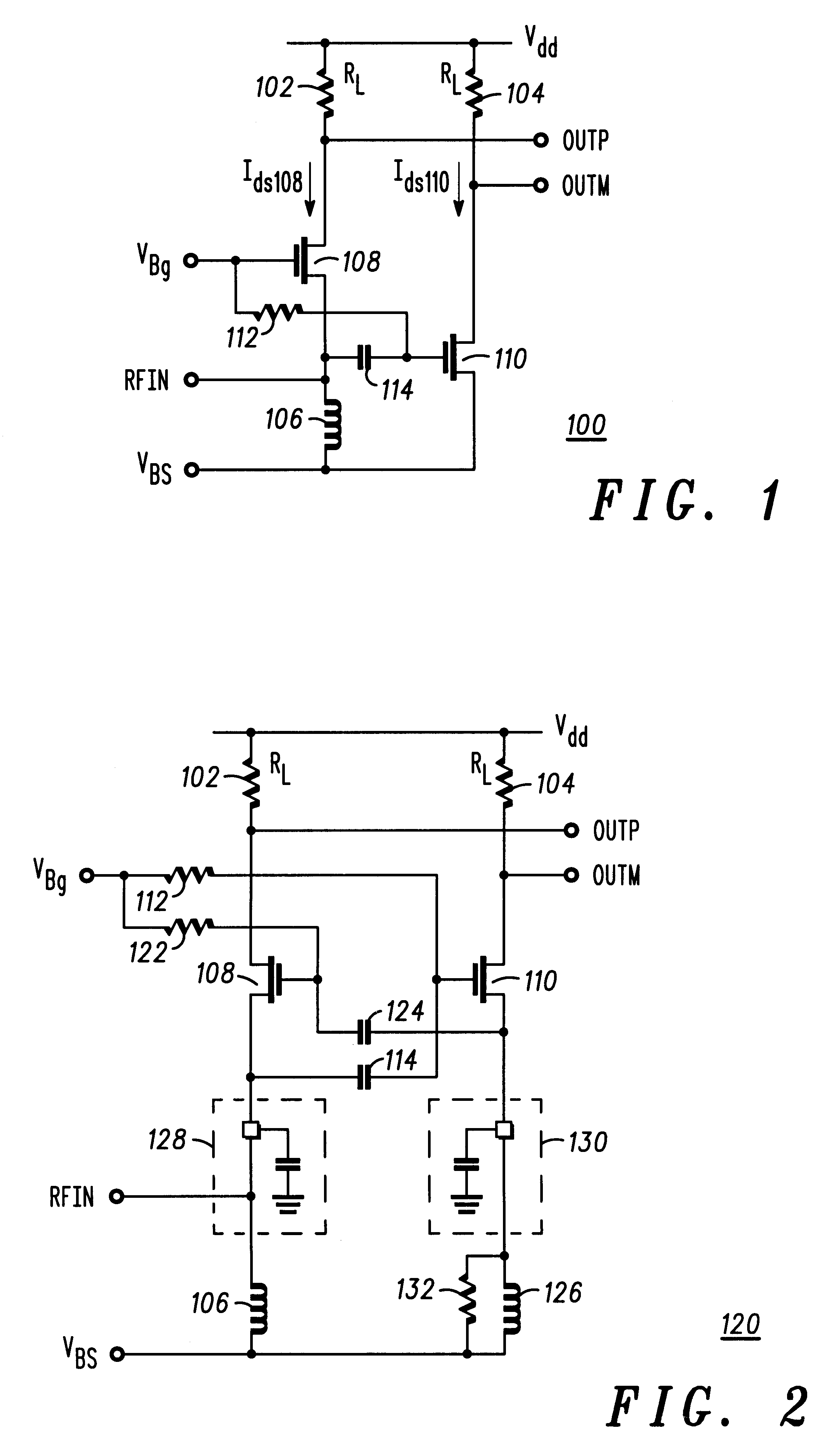
Turning now to the drawings, FIG. 1 schematically shows an example of a first embodiment single ended input differential output amplifier 100 according to the present invention. A matched pair of load resistors 102, 104, typically 200.OMEGA. each, connect a supply voltage (V.sub.dd) to a corresponding differential output OUTP and OUTM. An inductor 106, typically 1000 nh, connects input RFIN to a reference voltage V.sub.BS. The bulk substrate for FETs 108, 110 is grounded. A first field effect transistor (FET) 108 (n-type in this example) connects, drain to source, between load resistor 102 at output OUTP and inductor 106 at RFIN. A second FET 110 (also n-type in this example) connects, drain to source, between the second load resistor 104 at output OUTM and the reference voltage V.sub.BS. A gate bias resistor 112, typically 50 k.OMEGA., connects between the gates of FETs 108, 110. A gate bias voltage (V.sub.Bg) connects to the gate of FET 108 and resistor 112. A coupling capacitor 1...


PUM


Abstract

A single ended input differential output amplifier (100) and integrated circuit including such an amplifier (100). A pair of load resistors (102, 104) are connected between a supply voltage (Vdd) and differential outputs OUTP and OUTM. An inductor (106) is connected between input RFIN and a source bias voltage VBS. A first field effect transistor (FET) (108) is connected, drain to source, between load resistor (102) at output OUTP and inductor (106) at RFIN. A second FET (110) is connected, drain to source, between the second load resistor (104) at output OUTM and the source bias voltage VBS. A gate bias voltage VBg is connected to the gate of FET (108) and through resistor (112) to the gate of FET (110). A coupling capacitor (114) is connected between the input RFIN and the gate of FET (110). The gate of FET (108) may be connected to gate bias voltage VBg through a second gate bias resistor (122) and a second coupling capacitor (124) may couple the source of FET (110) to the gate of FET (108), thereby providing common mode rejection for noise, e.g., substrate noise, experienced at inductor (106).

Description

1. Field of the InventionThe present invention is related to wide band linear amplifiers and more particularly to resistively loaded wide-band high frequency linear amplifiers with a single ended input and a differential output.2. Background DescriptionWide band multi-channel communication systems require wide band amplifiers with a high degree of linearity to avoid second and third order affects arising from a large number of potential carrier interactions. Traditional wide band amplifiers require very expensive external tracking filters, e.g., an external balun. Thus, because differential circuits and in particular differential circuits with external baluns minimize second and third order effects, they are used, overwhelmingly, in high performance narrow band applications to maximize amplification linearity.For many applications an external balun or other tracking filter is prohibitively expensive and, an on-chip single ended (single phased) input to differential (output) converte...

Claims


Application Information

Patent Timeline
Patent Type & Authority Patents(United States)
IPC IPC(8): H03F3/189H03F3/193
CPCH03F3/193
Inventor HOLLENBECK, NEAL W.CONNELL, LAWRENCE EDWIN
Owner NXP USA INC
Why Eureka
Try Eureka