

Semiconductor storage device
a technology of semiconductors and storage devices, applied in semiconductor devices, electrical equipment, transistors, etc., can solve the problem of needing to reduce the area of sram cells further
- Summary
- Abstract
- Description
- Claims
- Application Information
AI Technical Summary
Benefits of technology
Problems solved by technology
Method used
Image

Examples
first embodiment
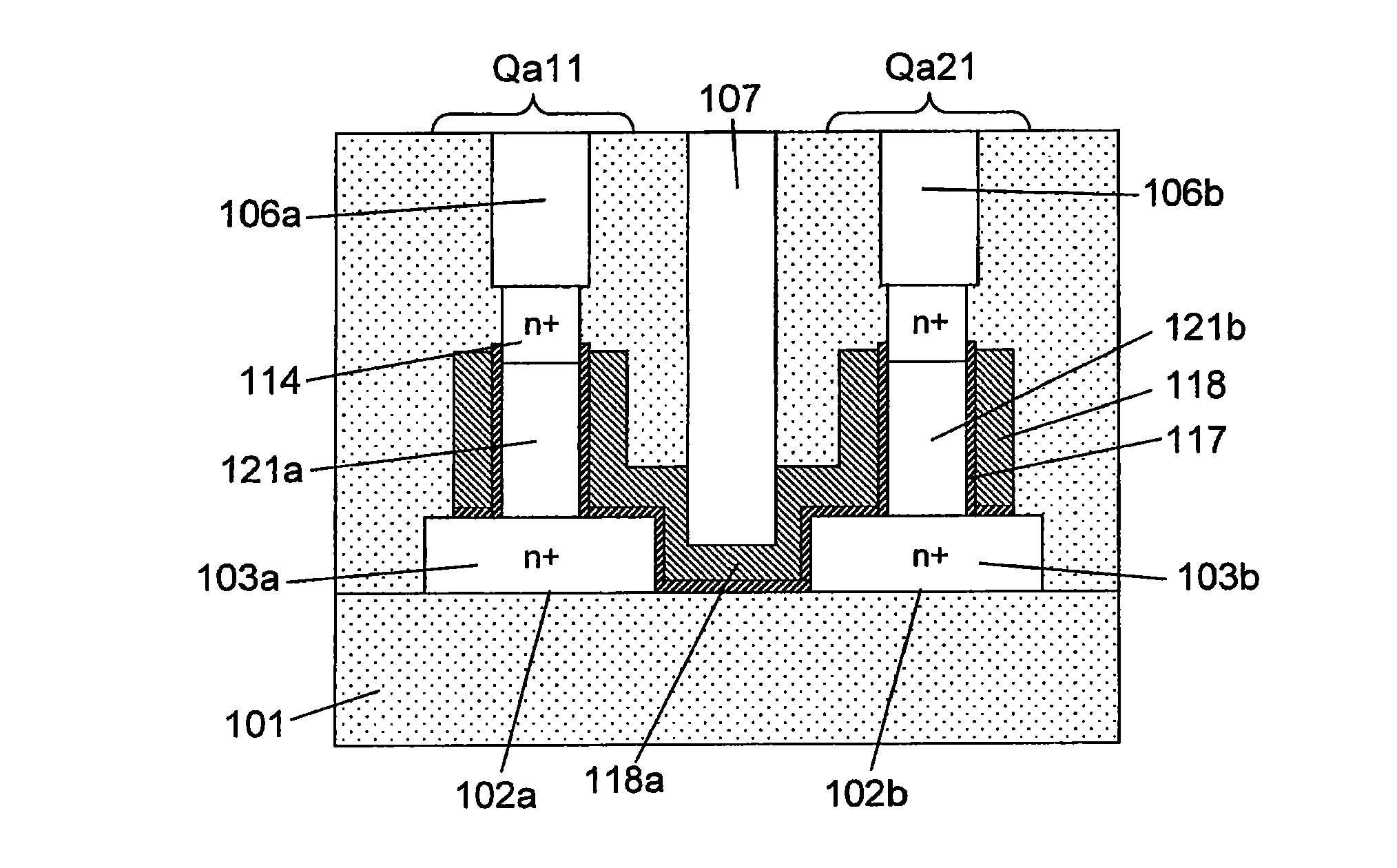
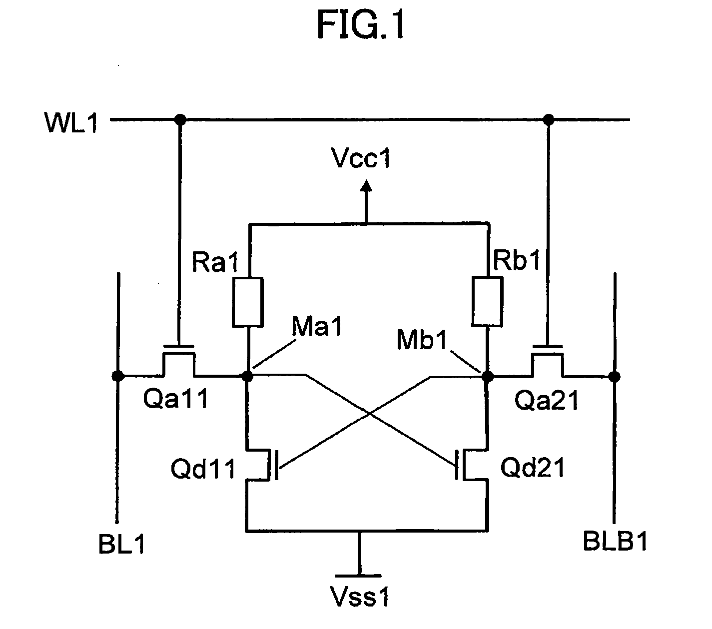
[0044]FIG. 1 illustrates an equivalent circuit of a memory cell in an E / R type 4T-SRAM according to a first embodiment of the present invention. In FIG. 1, each of BL1 and BLB1 indicates a bit line, and WL1 indicates a word line. Vcc1 indicates a power source potential, and Vss1 indicates a ground potential. Each of Qa11 and Qa21 indicates an access transistor operable to allow access to the memory cell, and each of Qd11 and Qd21 indicates a driver transistor operable to drive an after-mentioned storage node so as to read and write data from / to the memory cell. Each of Ra1 and Rb1 indicates a load resistor element for supplying electric charges to the after-mentioned storage node, and each of Ma1 and Mb1 indicates a storage node for storing data therein.
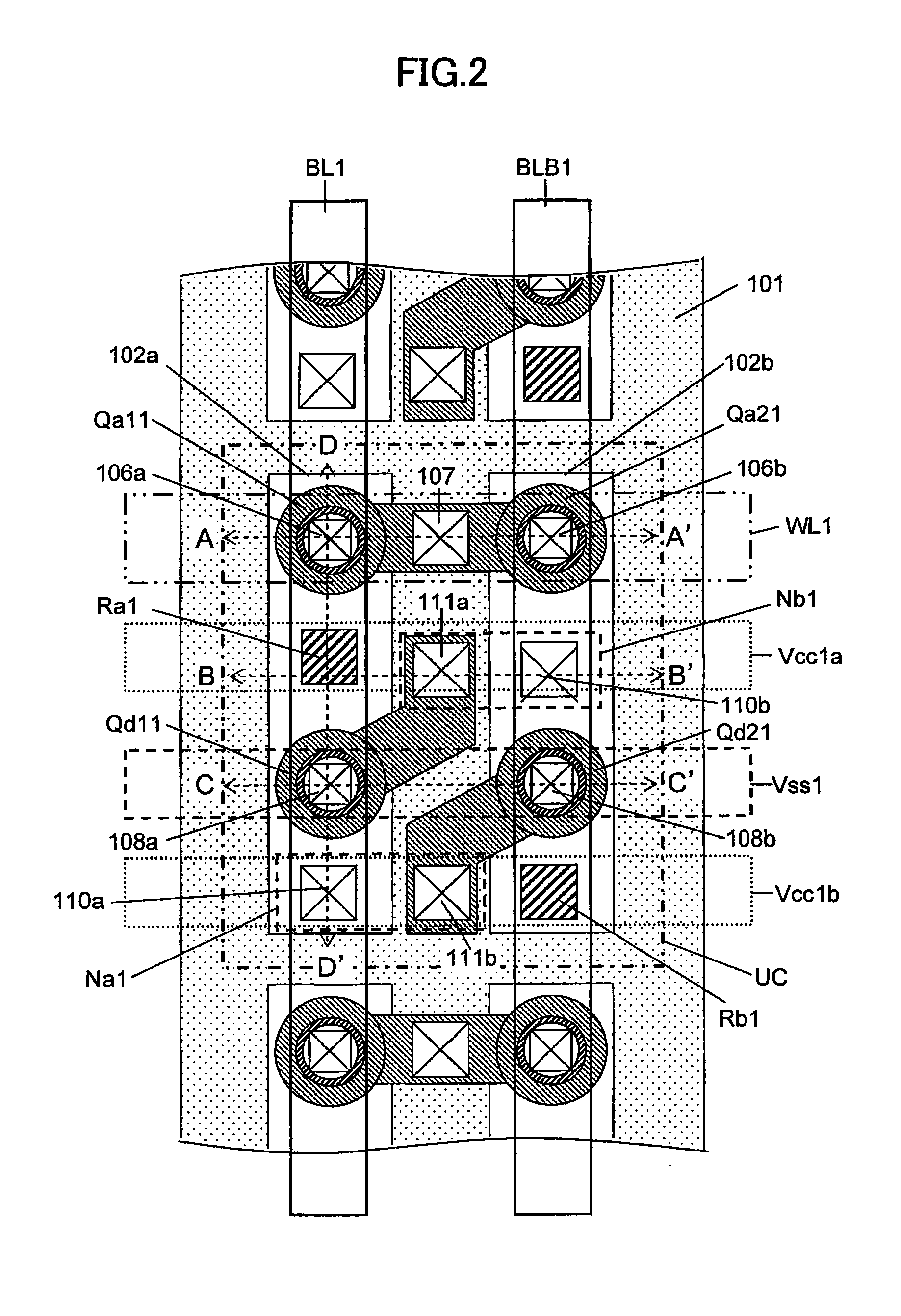
[0045]FIG. 2 illustrates a layout of the memory cell in the SRAM according to the first embodiment. In an SRAM cell array, a unit cell illustrated in FIG. 2 is iteratively arranged. FIGS. 3(a) to 3(d) are sectional views taken along ...
second embodiment
[0080]FIG. 16 illustrates a layout of a memory cell in an SRAM according to a second embodiment of the present invention. The second embodiment is different from the first embodiment in the following respect. A planar silicon layer 202a serving as a storage node is connected to a gate line extending from a gate electrode of a driver transistor Qd22, through a common contact 210a formed to extend thereacross, and a planar silicon layer 202b serving as a storage node is connected to a gate line extending from a gate electrode of a driver transistor Qd12, through a common contact 210b formed to extend thereacross. As above, the gate and the storage node are connected to each other through the contact, instead of an interconnection layer, so that the number of contacts in the SRAM cell can be reduced. Thus, a cell area can be reduced by adjusting an arrangement of pillar-shaped silicon layers and contacts.
[0081]As mentioned in the first embodiment, in order to share each of the word lin...
third embodiment
[0083]FIG. 17 illustrates a layout of a memory cell in an SRAM according to a third embodiment of the present invention. In the third embodiment, an arrangement of two transistors arrayed in the 1st column of a unit cell UC illustrated in FIG. 17 in an SRAM cell array is identical to that of two transistors arrayed in the 2nd column in a memory cell adjacent to and on an upper or lower side of the unit cell UC, and an arrangement of two transistors arrayed in the 2nd column of the unit cell UC is identical to that of two transistors arrayed in the 1st column in the memory cell adjacent to and on the upper or lower side of the unit cell UC. Specifically, two transistors are arrayed on the upper side of transistors Qa13, Qd13 arrayed in the 1st column of the unit cell UC in FIG. 17, in the same arrangement as that of transistors Qa23, Qd23 arrayed in the 2nd column of the unit cell UC in FIG. 17, in this order in a downward direction. Thus, in FIG. 17, an access transistor is disposed...
PUM
 Abstract
Description
Claims
Application Information