Methods and apparatus for a composite collector double heterojunction bipolar transistor

a bipolar transistor and composite collector technology, applied in the field of improved heterojunction bipolar transistors, can solve the problems of unsatisfactory known dhbts in a number of respects, devices with high knee voltage tend to be less efficient, and devices with high knee voltage often exhibit high voltag

a bipolar transistor and composite collector technology, applied in the field of improved heterojunction bipolar transistors, can solve the problems of unsatisfactory known dhbts in a number of respects, devices with high knee voltage tend to be less efficient, and devices with high knee voltage often exhibit high voltag

US6563145B1Inactive Publication Date: 2003-05-13SKYWORKS SOLUTIONS INC

Image

  • Methods and apparatus for a composite collector double heterojunction bipolar transistor
  • Methods and apparatus for a composite collector double heterojunction bipolar transistor
  • Methods and apparatus for a composite collector double heterojunction bipolar transistor

Examples


Embodiment Construction

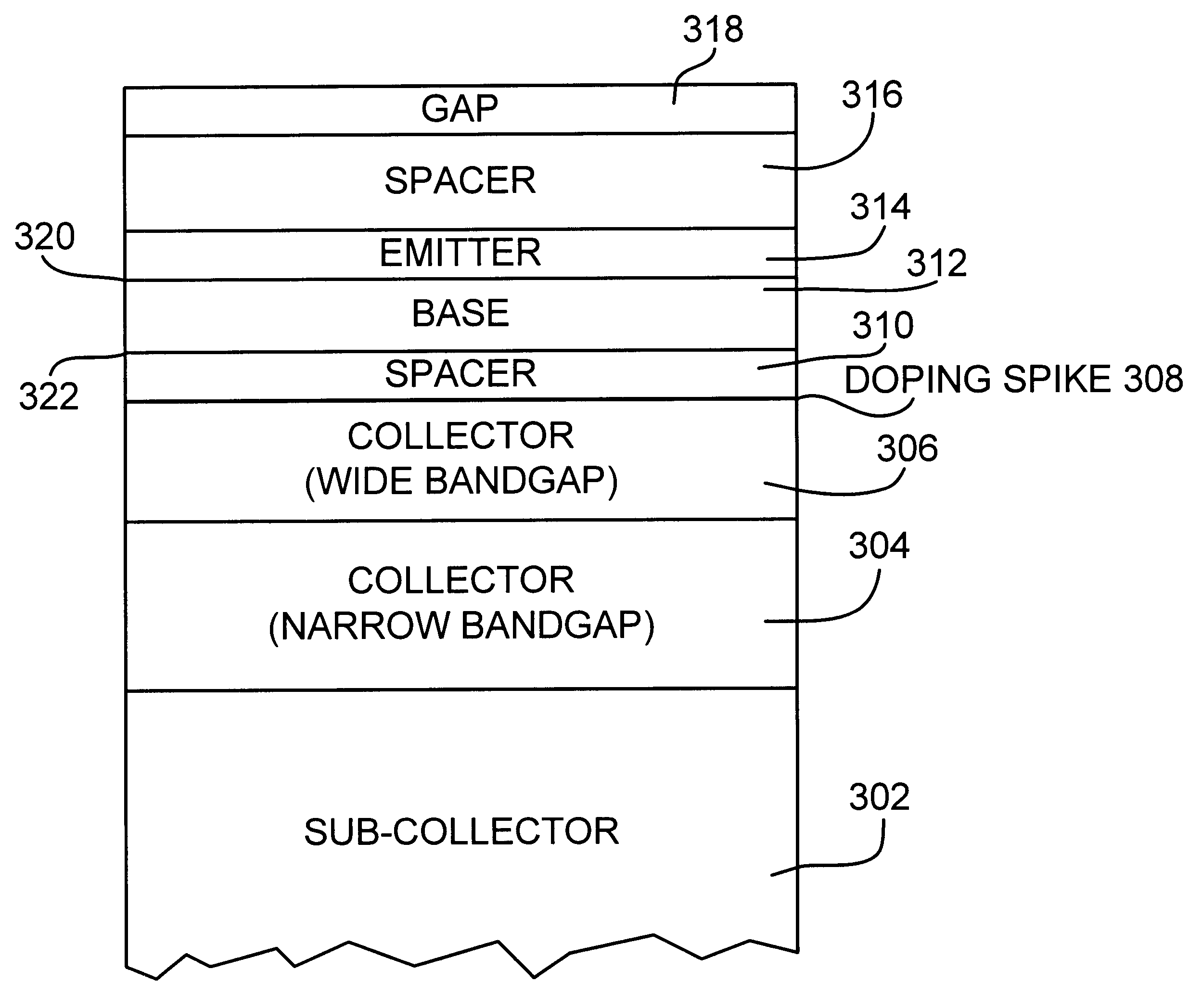
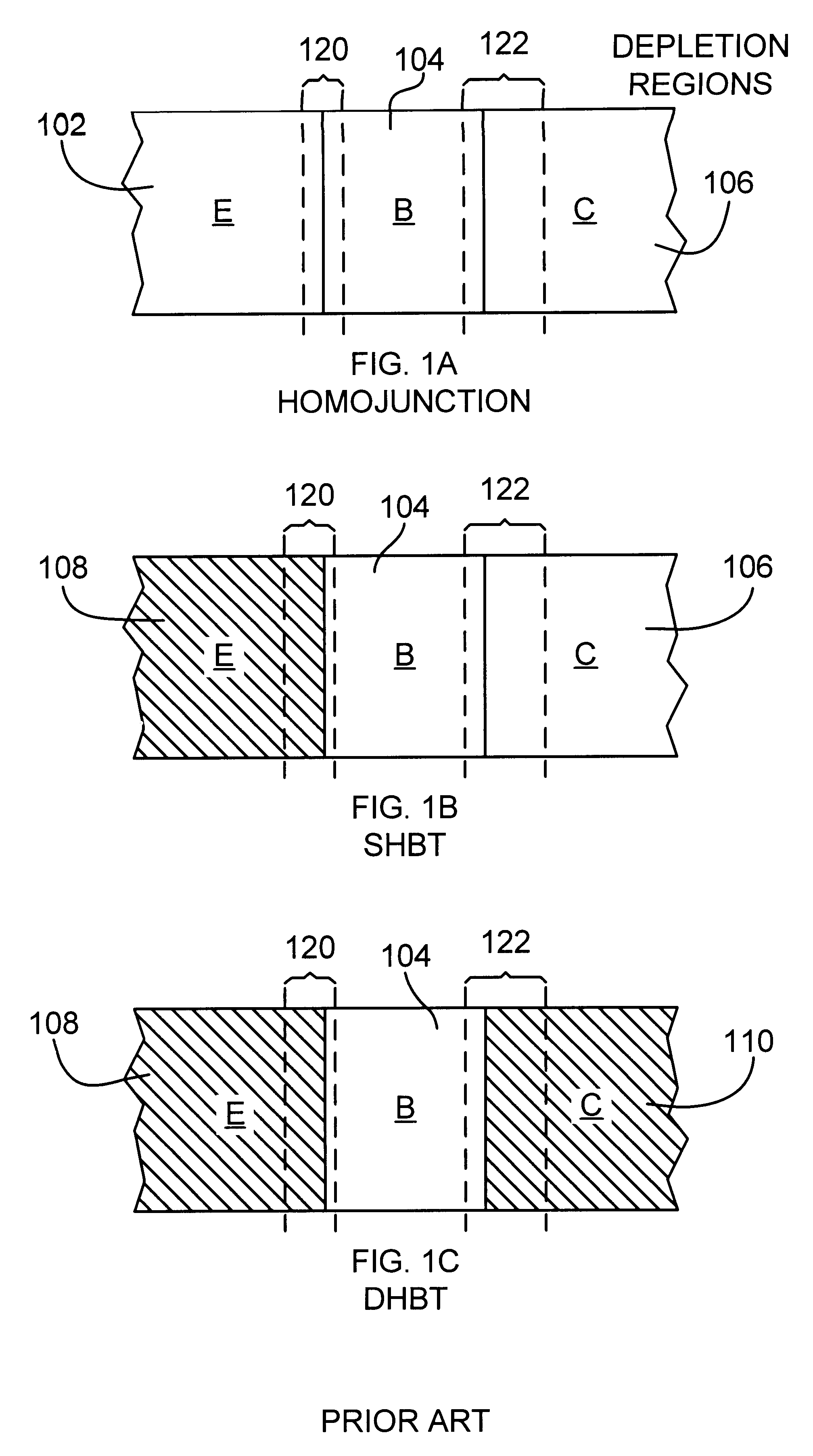
Systems and methods in accordance with various aspects of the present invention provide a composite collector double heterojunction bipolar transistor (CCHBT) which incorporates a first material in the area of highest electric field, and a second material for the rest of the collector, wherein the first material can support high electric fields and has low mobility, and the second material exhibits high mobility (e.g., less resistance) but may not support high fields. In a preferred embodiment, as set forth below, the first material comprises a wide bandgap semiconductor, and the second material comprises a narrow bandgap semiconductor. In this way, breakdown voltage is increased and, at the same time, knee-voltage, and offset voltage are reduced. By way of contrast, in known DHBTs, the wide-to-narrow bandgap material transition occurs a significant distance from the active collector region (outside the depletion region), and therefore suffers from many of the limitations addressed ...


PUM


Abstract

A compound collector double heterojunction bipolar transistor (CCHBT) incorporates a collector comprising two layers: a wide bandgap collector region (e.g., GaAs), and a narrow bandgap collector region (e.g., InGaP). The higher electric field is supported in the wide bandgap region, thereby increasing breakdown voltage and reducing offset voltage. At the same time, the use of wide bandgap material in the depleted portion of the collector, and a higher mobility material toward the end and outside of the depletion region, reduces series resistance as well as knee voltage.

Description

1. Technical FieldThe present invention relates, generally, to semiconductor devices and, more particularly, to an improved heterojunction bipolar transistor incorporating a compound collector structure.2. Background InformationIn contrast to a standard homojunction transistor, a heterojunction bipolar transistor (HBT) includes at least two dissimilar semiconductor materials. That is, referring now to FIGS. 1A and 1B, while the emitter 102, base 104, and collector 106 of a standard homojunction transistor are formed from the same semiconductor material (e.g., Si or GaAs), in a single heterojunction bipolar transistor (SHBT), the emitter 108 is formed from a wide bandgap material, and the base 104 is formed from a narrow bandgap material. For example, among the III-V compounds, Al.sub.x Ga.sub.l-x As (AlGaAs) may be used for the wide bandgap material, and a ternary compound such as GaAs may be used for the narrow bandgap material.Among other things, HBTs can achieve large gain values...

Claims


Application Information

Patent Timeline
13 May 2003
Publication
US6563145B1
IPC
H01L21/02; H01L21/331; H01L29/08; H01L29/66; H01L29/02; H01L29/737
CPC
H01L29/0821; H01L29/7371; H01L29/66318; H01L29/20
Inventors
CHANG, CHARLES E.; PIERSON, RICHARD L.