WDM transmitter or receiver including an array waveguide grating and active optical elements

a technology active optical elements, applied in the field of optical communication, can solve the problems of time-consuming, difficult, and time-consuming assembly work of array waveguide grating receiving inputs

Inactive Publication Date: 2003-07-15
PHOTONIC
View PDF22 Cites 40 Cited by
  • Summary
  • Abstract
  • Description
  • Claims
  • Application Information

AI Technical Summary

Problems solved by technology

A difficulty with the various devices shown in the Ishida patent is that the array waveguide grating receives inputs and couples its outputs to other devices through optical fibers.
This assembly work is particularly time consuming and difficult because the pigtailed fibers must be aligned carefully with the input optics of the array waveguide grating.
Assembling the devices shown in the Ishida patent is time consuming and undesirably increases the cost of the illustrated switches.
The expense of such switches presently limits the possibility of using such switches in many applications.
A similar problem arises when array waveguide gratings are used in combination with detectors to form an analyzer or a channel receiver.
Assembly of the illustrated devices requires considerable precise manual labor, undesirably increasing the cost of the components.

Method used


Image

  • WDM transmitter or receiver including an array waveguide grating and active optical elements
  • WDM transmitter or receiver including an array waveguide grating and active optical elements
  • WDM transmitter or receiver including an array waveguide grating and active optical elements

Examples


Embodiment Construction

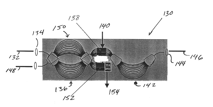
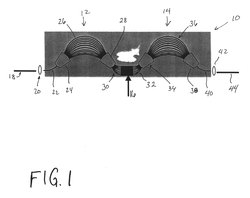
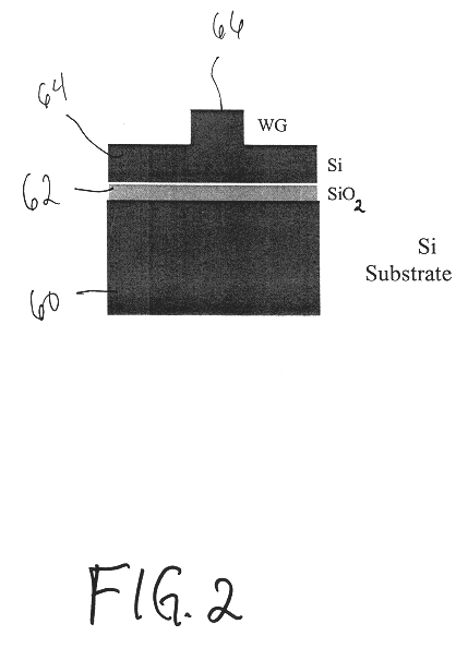
An aspect of the present invention provides an optical component with a substrate having one or more waveguide structures formed on a surface. The substrate comprises a first semiconductor material. An optical detector is bonded to a surface of a first of the waveguide structures and comprises a second semiconductor material different from the first semiconductor material and adapted so that light from the first waveguide structure is coupled into the optical detector and converted into an electrical signal.

Another aspect of the invention provides an optical component with a substrate having an plurality of waveguide structures formed on a surface, at least a portion of the array comprising substantially parallel waveguide structures. The substrate comprises a first semiconductor material. The component includes an array of optical detectors, each optical detector bonded to a surface of a corresponding one of the waveguide structures. The optical detectors comprise a second semicond...


PUM


Abstract

An optical component is formed on a silicon on insulator (SOI) substrate and has an array waveguide that demultiplexes an input light signal into N channels and provides that light signal to a corresponding set of N waveguide structures formed on a surface of the SOI substrate. The N waveguide structures provide the N channels of light to N optical detectors. Each optical detector is bonded to a surface of a corresponding one of the waveguide structures. The N channels of light pass through the N waveguide structures and are coupled into the N optical detectors so that light from a corresponding channel of the array waveguide is coupled into a corresponding optical detector and converted into an electrical signal.

Description

1. Field of the InventionThe present invention relates to optical communications of the type used in communication over optical networks and particularly relates to optical communications through fiber optic links using multiple wavelength or broad spectrum light for communication.2. Discussion of the Related ArtOptical communications networks have become prevalent in long distance communication networks, including for the backbone of the Internet. Demand for additional bandwidth in all manner of optical networks continues to grow and a variety of different strategies have been adopted to improve the utilization of the bandwidth within existing optical fiber networks. There is, for example, increasing utilization of multiple wavelength or broad-spectrum light communication over optical fiber links, generally using the technology known as wavelength division multiplexing ("WDM"). Presently the most common implementation of WDM communication uses a plurality of different lasers as lig...

Claims


Application Information

Patent Timeline
Patent Type & Authority Patents(United States)
IPC IPC(8): G02B6/34G02B6/42
CPCG02B6/12021G02B6/4249G02B6/12014
Inventor DUTT, BIRENDRACHAN, JAMES
Owner PHOTONIC
Why Eureka
Try Eureka