Method and apparatus for reducing PFC emission during semiconductor manufacture

Inactive Publication Date: 2003-08-05
SAMSUNG ELECTRONICS CO LTD
View PDF21 Cites 4 Cited by
  • Summary
  • Abstract
  • Description
  • Claims
  • Application Information

AI Technical Summary

Benefits of technology

Other features and advantages of the present invention will become apparent to those skilled in the art from the following detailed description. It is to be understood, however, that the detailed description and specific examples, while indicating preferred embodiments of the present invention, are given by way of illustration and not limitation. Many changes and modifications within the scope of the present invention may be made without departing from the spirit thereof, and the invention includes all such modifications.

Problems solved by technology

Such processes, however, are expected to increase the overall cost of the semiconductor manufacturing process.
Furthermore, it may be difficult to integrate the various abatement scrubbers into existing process layouts and to maintain the scrubbers once they are installed.
Furthermore, the amounts of PFC's actually recycled typically is small due to the small amounts of PFC's that are captured.
Moreover, if recycling proves impossible, another system must be employed to dispose of the captured PFC's.
Use of alternative process gases and process optimization have also proven problematic due to the insufficiency of suitable alternative gases and low process yield.

Method used


Image

  • Method and apparatus for reducing PFC emission during semiconductor manufacture
  • Method and apparatus for reducing PFC emission during semiconductor manufacture
  • Method and apparatus for reducing PFC emission during semiconductor manufacture

Examples


first embodiment

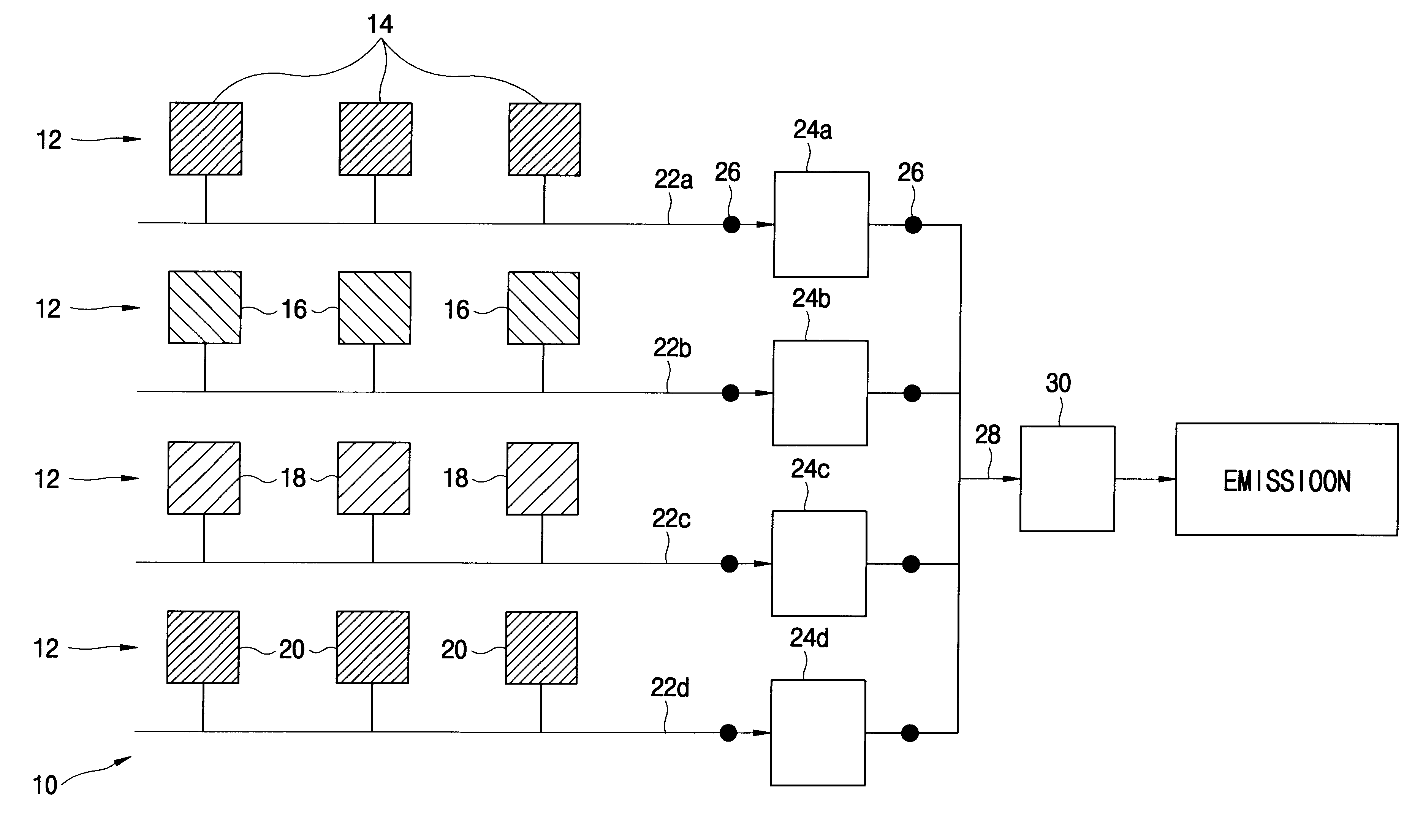
FIG. 3 is a schematic representation of a PFC emission reduction method of the invention, in which each separate sub-process of the overall semiconductor manufacturing process (e.g., oxide etching, poly etching, metal etching, chemical vapor deposition (CVD)) includes one or more individual devices, or tools, and emissions from each sub-process are received by a common exhaust line leading to a PFC abatement system dedicated to that sub-process, after which the exhausts from each PFC abatement system are combined and fed to a common wet scrubbing system,

second embodiment

FIG. 4 is a schematic representation of a PFC emission reduction method of the invention, in which emissions from dry etchers used in each dry etching sub-process are combined and directed to a first PFC abatement system, while emissions from CVD reactors used in a CVD sub-process are directed to a second PFC abatement system, after which the exhausts from the first and second PFC abatement systems are combined and fed to a common wet scrubbing system, and

FIGS. 5-7 are illustration of exemplary PFC abatement systems that can be employed in particular embodiments of the inventive method and apparatus.

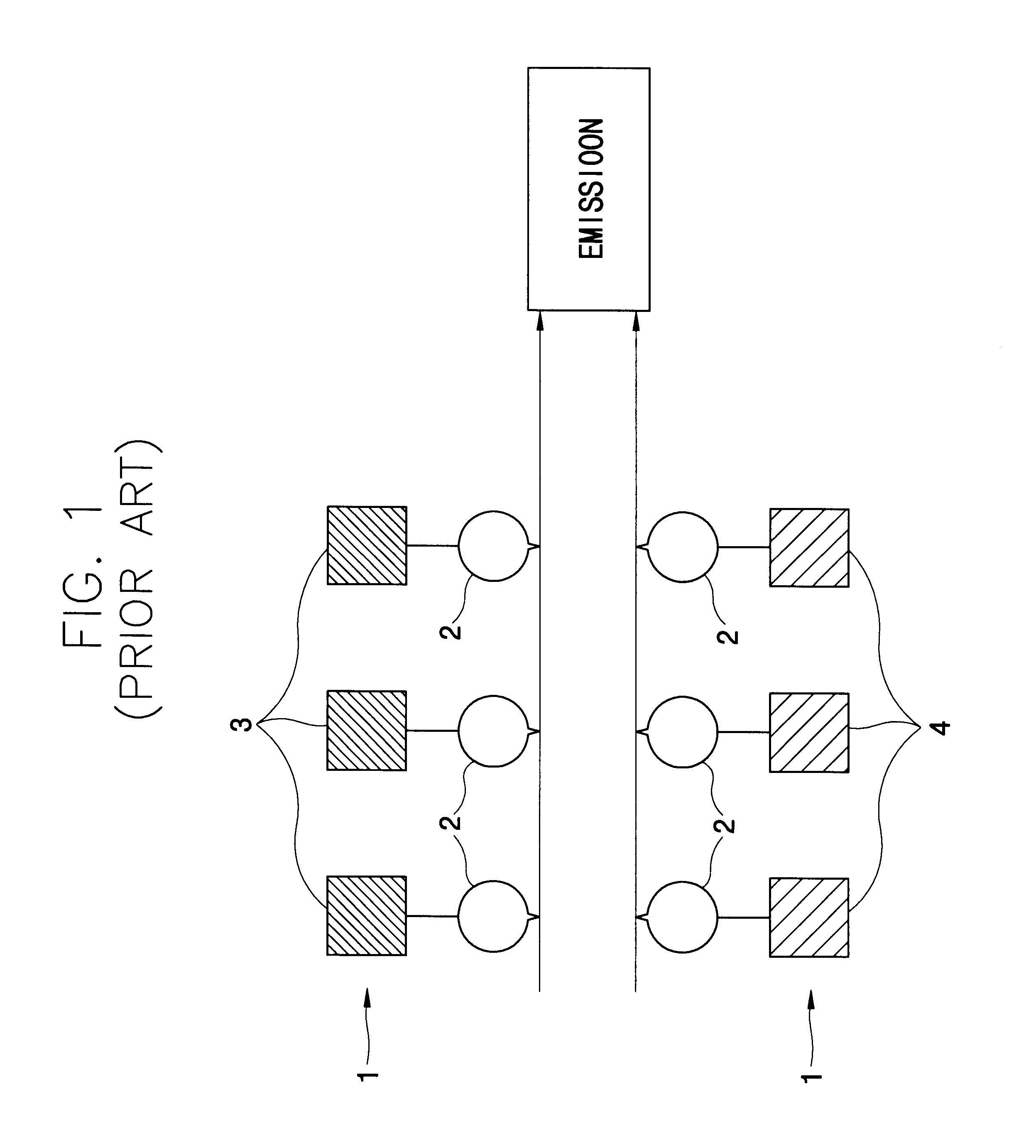
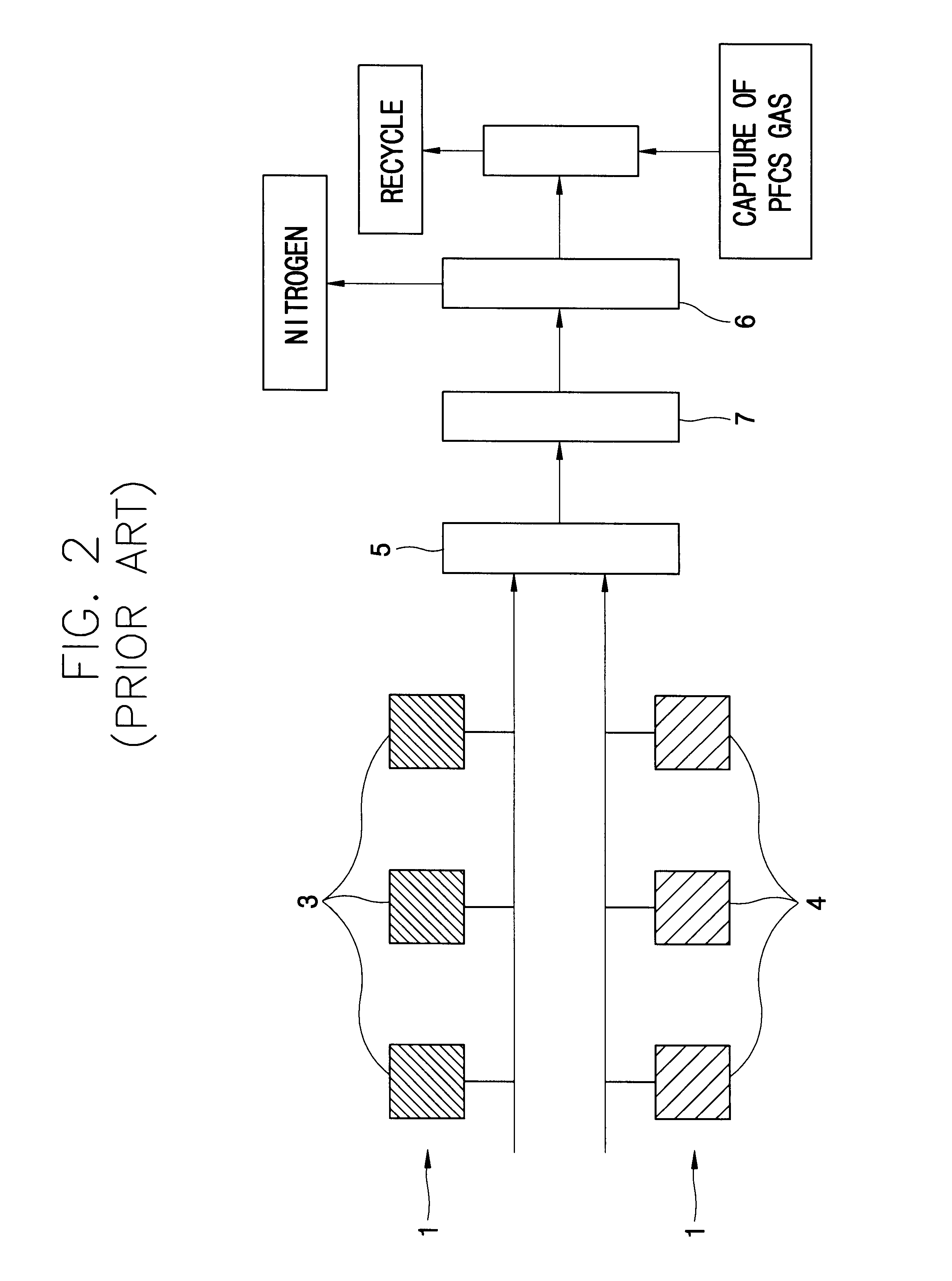
According to a first particular embodiment of the invention exemplified by FIG. 3, a system 10 for reducing PFC emissions during semiconductor manufacture includes a plurality of sub-process devices 12, for example without limitation, a first plurality of oxide etchers 14, a second plurality of poly etchers 16, a third plurality of metal etchers 18, and a fourth plurality of CVD reactors...


PUM

PropertyMeasurementUnit
Wettabilityaaaaaaaaaa

Abstract

A method of reducing PFC emissions during a semiconductor manufacturing process that includes a set of sub-processes each of which produces at least one PFC includes the steps of exhausting PFC's produced by each sub-process to a common line to form a combined exhaust stream, treating the combined exhaust stream from each sub-process using a separate PFC abatement system, combining the treated exhaust streams to form a combined treated stream, and wet scrubbing the combined treated stream.

Description

1. Field of the InventionThe present invention relates to a method and system for reducing the emission of PFC's (perfluoro compounds) during semiconductor manufacturing processes.2. Background of the InventionEffluent gases emitted during semiconductor manufacturing processes, for example during CVD chamber cleaning and dry etch processes, frequently contain perfluoro compounds (PFC's). PFC's are global warming gases, and significant efforts have been and are continuing to be made to reduce and minimize the amount of PFC's that are emitted into the atmosphere. In particular, a convention of the World Semiconductor Council, including the United States, Europe, Japan, Taiwan and Korea, seeks to reduce the amount of PFC emission by 10% by the year 2010, with the following basis years: United States, Europe, Japan: 1995; Korea: 1997; Taiwan: 1998.Known procedures for reducing the amount of PFC emission include use of abatement scrubbers, capture and recycle, use of alternative process ...

Claims


Application Information

Patent Timeline
IPC IPC(8): B01D53/70B01D53/68B01D53/34B01D53/77C23C16/44H01L21/205H01L21/302H01L21/3065
CPCB01D53/70B01D2257/2066Y02C20/30Y02P70/50
Inventor CHAE, SEUNG-KILEE, SANG-GONCHUNG, SANG-HYUKHEO, SEONG-JIN
Owner SAMSUNG ELECTRONICS CO LTD
Why Eureka
Try Eureka