Method and circuit for dynamic calibration of flash analog to digital converters

a technology of flash analog and digital converter, applied in the field of electronic circuits, can solve the problems of not addressing the dynamic offset or dynamic gain of the full adc under normal operating conditions, adding design time, space, and manufacturing cos

Inactive Publication Date: 2003-08-05
IBM CORP
View PDF12 Cites 84 Cited by
  • Summary
  • Abstract
  • Description
  • Claims
  • Application Information

AI Technical Summary

Problems solved by technology

This method accomplishes calibration of the DC offset and DC gain, but does not address the dynamic offset or dynamic gain of the full ADC under normal operating conditions, which includes the clocking of the ADC back end.
Thus, a separate precision analog comparator that adds design time, space, and manufacturing cost is needed.
Therefore, this method cannot be used to correct the overall gain or overall offset of the ADC.

Method used


Image

  • Method and circuit for dynamic calibration of flash analog to digital converters
  • Method and circuit for dynamic calibration of flash analog to digital converters
  • Method and circuit for dynamic calibration of flash analog to digital converters

Examples


Embodiment Construction

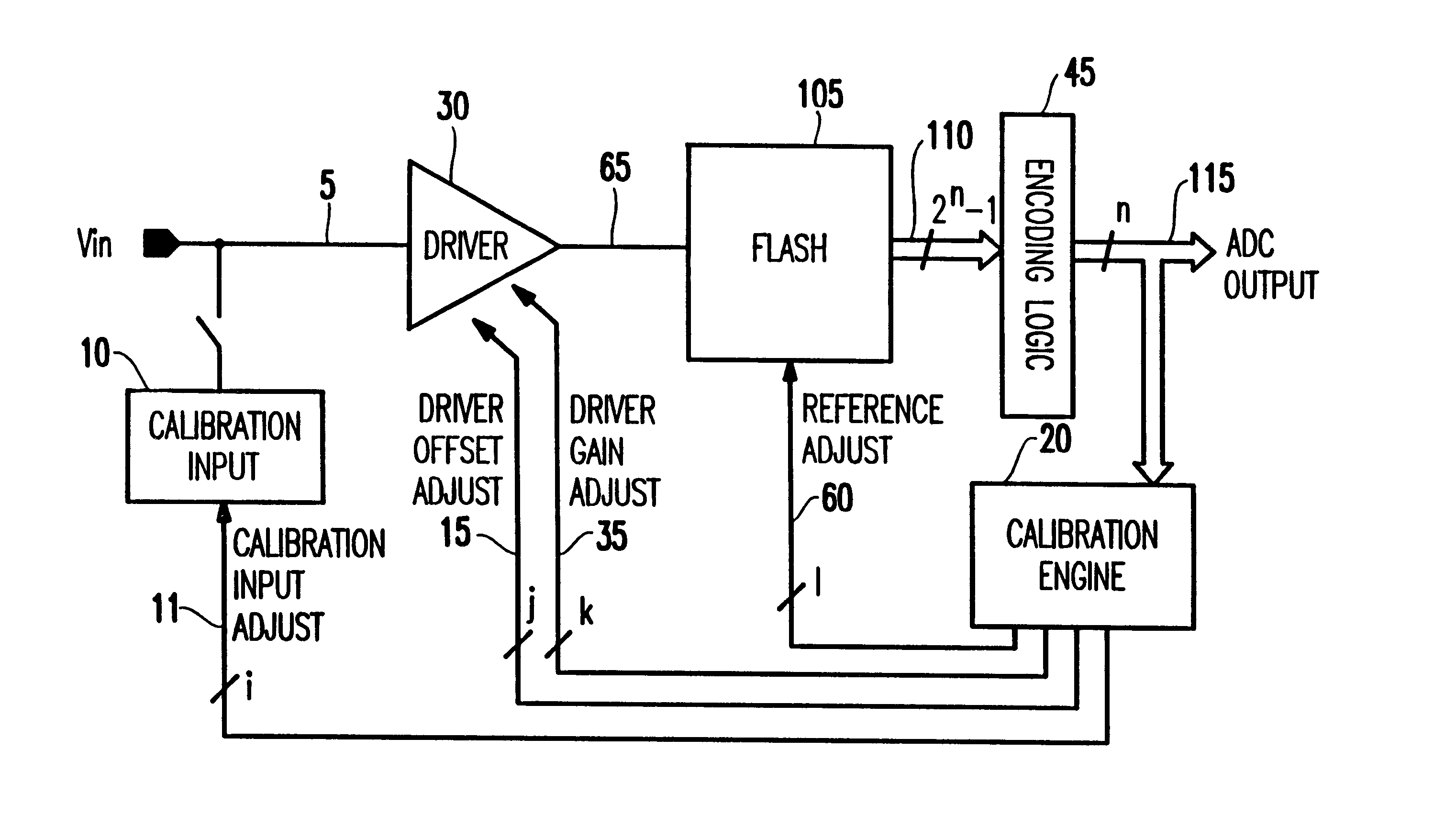
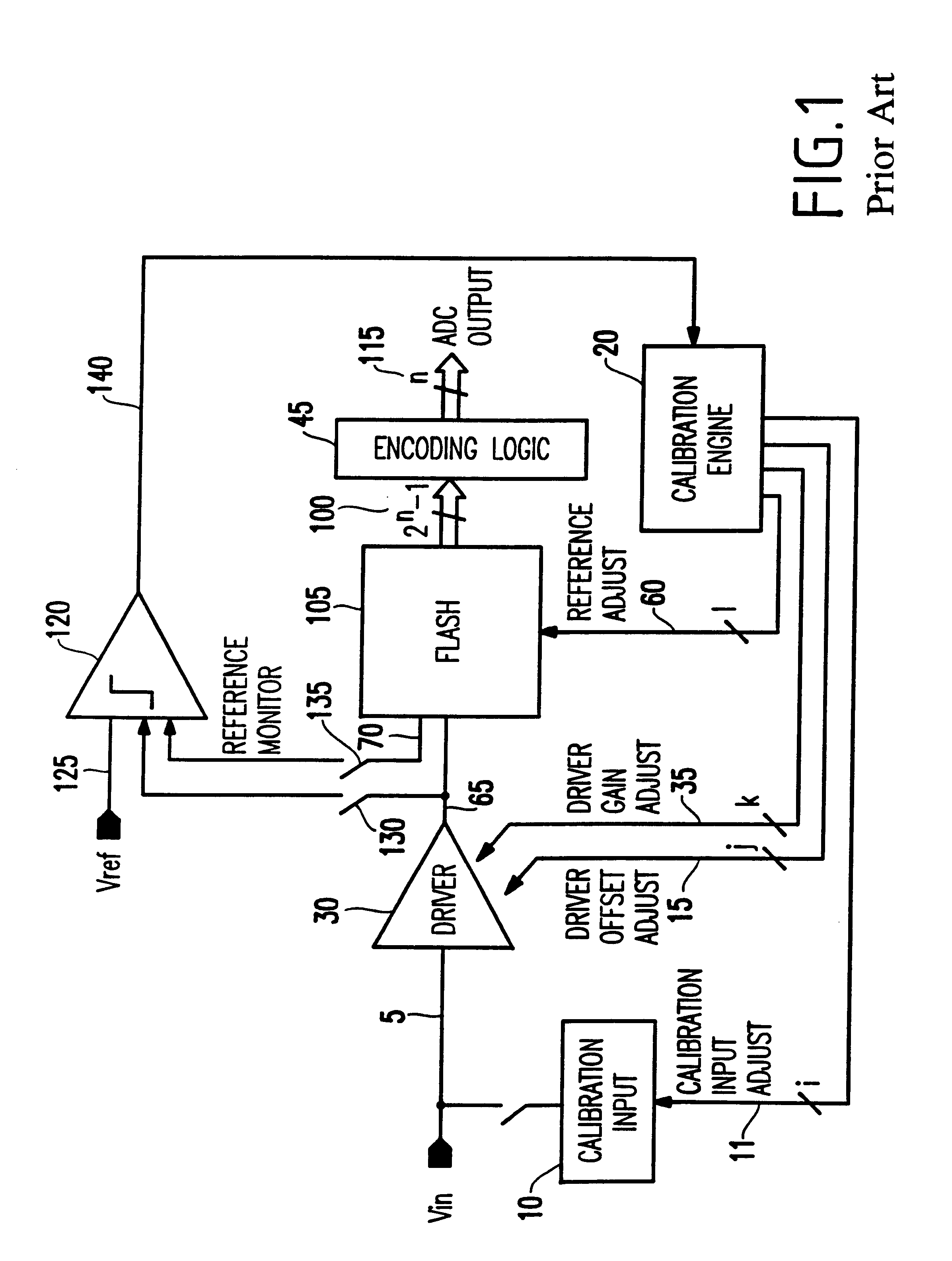
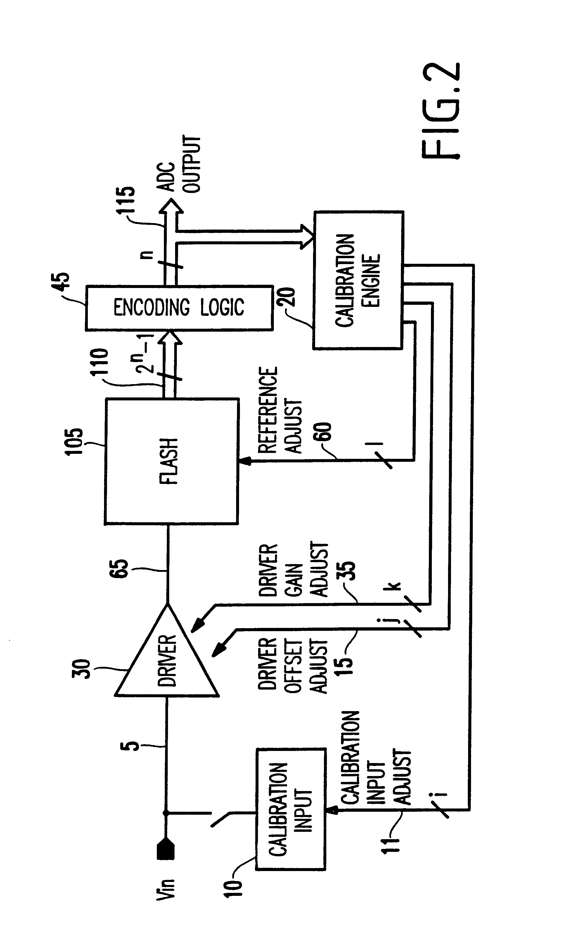
As previously mentioned, there is a need for a new and improved circuit and method for dynamic calibration of flash analog to digital converters as an entire system or unit. The new and improved circuit and method includes calibration of the overall gain and overall offset of the analog to digital converter system, as opposed to the gain or offset of individual component circuits separated out from the system. Further, the system is calibrated under the clocked conditions of normal operation, and the binary encoded output codes that are the normal output of the system are coupled as inputs into the calibration engine that drives the calibration. Conventional methods utilize a generic calibration engine for calibrating the analog circuits on a chip, where the output of an analog circuit is coupled into a separate precision analog comparator that functions only during calibration. During calibration of the analog circuit, the output of the precision analog comparator is fed into the i...


PUM


Abstract

A method and structure for calibrating an analog to digital converter comprises an input signal; a driver receiving the input signal, wherein the driver outputs a driver output signal; a flash circuit receiving the driver output signal, wherein the flash circuit outputs a comparison result equaling 2n-1 digital outputs; an encoding logic unit encoding the comparison result into n digital bits as an output signal; a calibration engine outputting a calibration input adjust signal, a reference adjust signal, a driver gain adjust signal, a driver offset adjust signal; and a calibration input circuit receiving the calibration input adjust signal, wherein the driver receives the driver gain adjust signal and the driver offset adjust signal, wherein the flash circuit receives the reference adjust signal, wherein the calibration engine receives n digital bits, and controls an operation of the driver or flash circuit based on the output signal.

Description

1. Field of the InventionThe present invention generally relates to electronic circuits designed for semiconductor integrated circuit manufacturing, and more particularly to an electronic circuit for dynamically calibrating an analog to digital converter.2. Description of the Related ArtLow voltage all CMOS flash Analog to Digital Converters (ADC) face the competing requirements of speed and accuracy. On one hand, conversion rates are in the multi-Gigasample per second range. On the other hand, decreasing power supply voltages require that comparators must discriminate between analog signals separated by mere millivolts. As a result, the small device sizes required and the process variations associated with semiconductor integrated circuit manufacturing necessitate the need for the calibration of Analog to Digital Converters for gain, offset, and symmetry to minimize non-idealities.Calibration has typically been accomplished with the clocked portion of the flash ADC held in a fixed ...

Claims


Application Information

Patent Timeline
Patent Type & Authority Patents(United States)
IPC IPC(8): H03M1/10H03M1/36
CPCH03M1/1033H03M1/36
Inventor MASENAS, CHARLES J.MITCHELL, CHAD E.TANGHE, STEVEN J.VON BRUNS, SHARON L.
Owner IBM CORP
Why Eureka
Try Eureka