Method for inspecting a polishing pad in a semiconductor manufacturing process, an apparatus for performing the method, and a polishing device adopting the apparatus

a semiconductor manufacturing process and polishing pad technology, applied in the direction of lapping machines, instruments, abrasive surface conditioning devices, etc., can solve the problems of difficult to achieve accurate measurement, reduce the production yield of semiconductor devices, and take a long time to inspect the polishing pad 10 with the naked ey

Inactive Publication Date: 2003-11-18
INST FR DU PETROLE +1
View PDF12 Cites 12 Cited by
  • Summary
  • Abstract
  • Description
  • Claims
  • Application Information

AI Technical Summary

Benefits of technology

Another object of the present invention is to provide an apparatus for inspecting the polishing pad so as to reduce wafer defects during the polishing process.
The polishing pad is preferably inspected for defects before the polishing pad is placed on the polishing device so as not to cause wafer defects while the inspection is being conducted. The operator can also choose to inspect the polishing pad for defects during any idle time of the polishing process, or after the polishing process. In this way, the operator can quickly take follow-up measures when a defect is found in the polishing pad. Accordingly, the wafer is prevented from being scratched during the polishing process.

Problems solved by technology

While the polishing process can planarize a large area of the wafer W, there is a drawback.
Such defects can lower the production yield of the semiconductor device.
However, checking the polishing pad 10 with the naked eye takes a lot of time, and it is difficult to attain an accurate measurement because of the vagaries inherent in a process requiring human intervention.
However, though the above apparatuses can improve the surface uniformity and control the thickness of the wafer, scratches may still be generated on the surface of the wafer.

Method used


Image

  • Method for inspecting a polishing pad in a semiconductor manufacturing process, an apparatus for performing the method, and a polishing device adopting the apparatus
  • Method for inspecting a polishing pad in a semiconductor manufacturing process, an apparatus for performing the method, and a polishing device adopting the apparatus
  • Method for inspecting a polishing pad in a semiconductor manufacturing process, an apparatus for performing the method, and a polishing device adopting the apparatus

Examples


Embodiment Construction

The present invention now will be described more fully with reference to the accompanying drawings, in which preferred embodiments of the invention are shown. The invention may, however, be embodied in many different forms and should not be construed as being limited to the embodiments set forth herein; rather, these embodiments are provided so that this disclosure will be thorough and complete, and will fully convey the concept of the invention to those skilled in the art. In the drawings, the thickness of layers and regions are exaggerated for clarity.

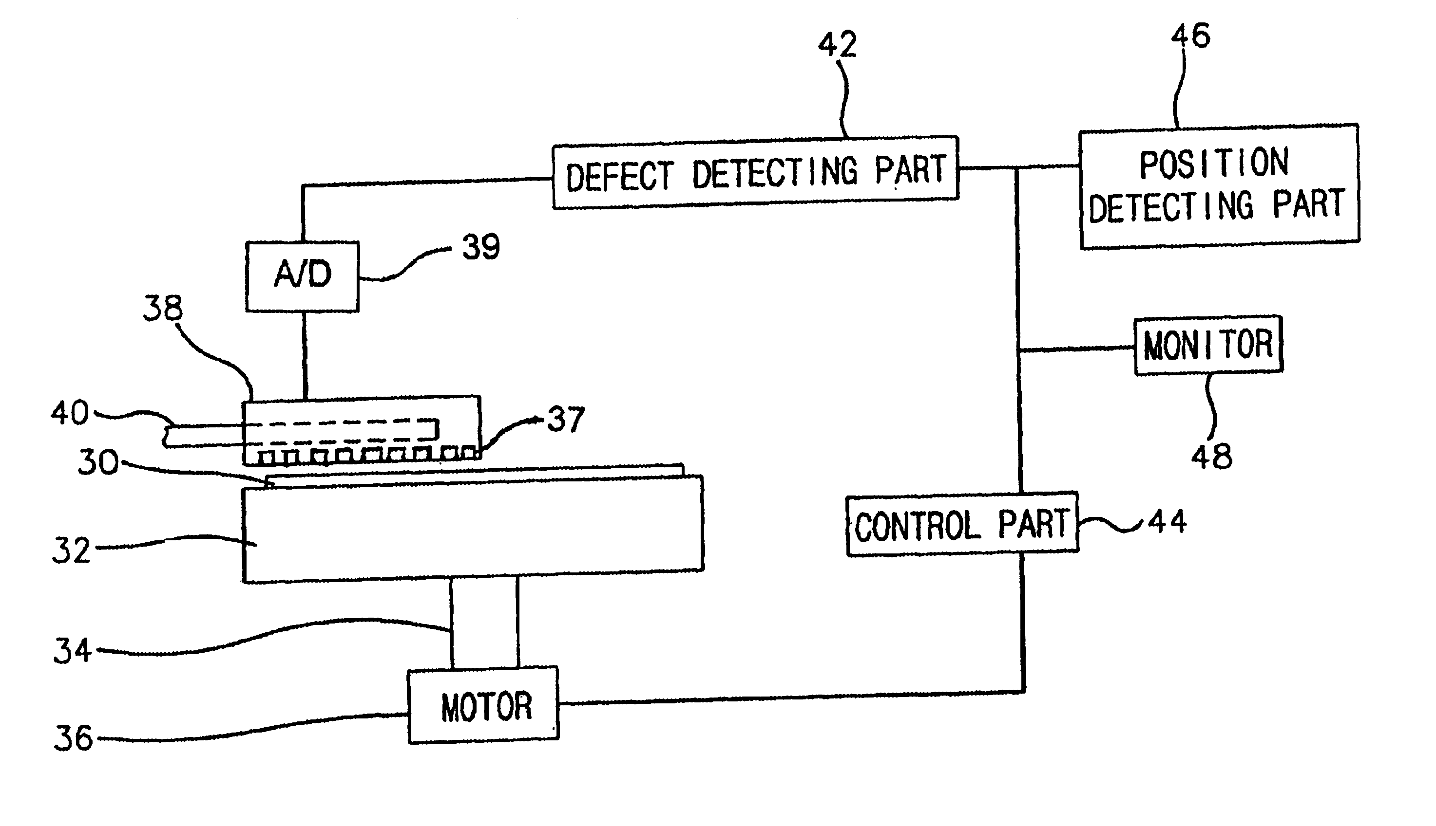
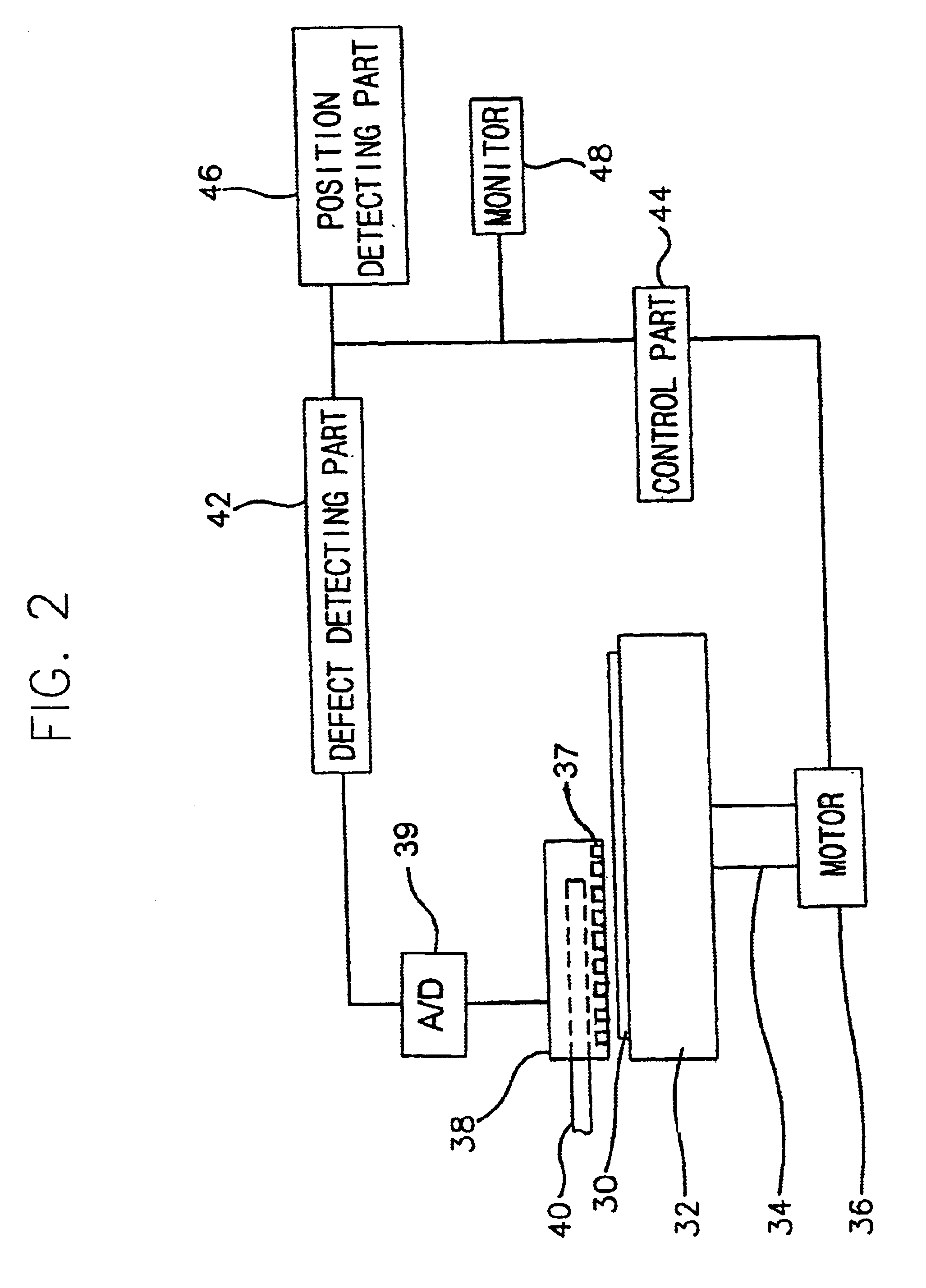
FIGS. 2 and 3 illustrate an apparatus for inspecting a polishing pad according to an embodiment of the present invention. FIG. 2 is a schematic view showing the structure of an apparatus for inspecting the polishing pad, and FIG. 3 is a plan view showing the apparatus for inspecting the polishing pad.

Referring to FIGS. 2 and 3, the polishing pad 30 is placed on a stage 32. A rotating shaft 34, positioned at a lower portion of the sta...


PUM

PropertyMeasurementUnit
areaaaaaaaaaaa
opticalaaaaaaaaaa
rotational angleaaaaaaaaaa

Abstract

A method for inspecting a polishing pad, an apparatus for performing the method, and a polishing device adopting the apparatus for preventing wafer defects. Polishing pad defects are detected by comparing optical data from a normal polishing pad, which does not cause wafer defects, with optical data from a polishing pad to be inspected. The respective optical data are obtained by radiating a beam into the polishing pad and then collecting and analyzing a beam reflected from the polishing pad.

Description

1. Field of the InventionThe present invention relates to a method for inspecting a polishing pad, an apparatus for performing the method of inspecting, and a polishing device adopting the apparatus, which can prevent wafer defects during wafer polishing operations.2. Description of the Related ArtDuring a conventional semiconductor manufacturing procedure, processes such as lithography, light exposure, ion implantation, chemical and mechanical polishing, chemical or physical deposition, and plasma etching, are performed on wafers to form semiconductor chips and devices. In particular, chemical and mechanical polishing processes are widely used for manufacturing the semiconductor device, because the chemical and mechanical polishing process can be carried out at a low temperature and a large area of the wafer can be planarized.FIG. 1 shows a conventional polishing device for manufacturing a semiconductor device. In FIG. 1, a platen 12 is provided with a polishing pad 10 which makes ...

Claims


Application Information

Patent Timeline
Patent Type & Authority Patents(United States)
IPC IPC(8): B24B37/04B24B49/12G01N21/88G01N21/95B24B37/20H01L21/66B24B37/24B24B49/00B24B53/017H01L21/304
CPCB24B37/013G01N21/9501B24B49/12H01L22/00
Inventor JUN, CHUNG-SAMKIM, KYE-WEONYANG, YU-SINKIM, HYO-HOO
Owner INST FR DU PETROLE
Why Eureka
Try Eureka