
Polishing pad and method of fabricating semiconductor device using the same

a technology of polishing pad and semiconductor substrate, which is applied in the direction of grinding/polishing apparatus, grinding machine, manufacturing tools, etc., can solve the problems of reducing the size of individual chips, increasing the complexity of the pattern of each layer, and reducing the polishing process. , to achieve the effect of reducing the number of defects on the semiconductor substrate during the polishing process

Pending Publication Date: 2022-03-31
SK ENPULSE CO LTD
View PDF0 Cites 0 Cited by
  • Summary
  • Abstract
  • Description
  • Claims
  • Application Information

AI Technical Summary

Benefits of technology

The patent describes a polishing layer used in the semiconductor industry that exhibits appropriate hardness and elongation for polishing various layers on a semiconductor substrate during a polishing process. The polishing layer has a tensile strength of 18 N / mm2 to 22 N / mm2 and a hardness (Shore D) of 35 to 55. The polishing layer has a narrow molecular weight distribution, resulting in a desired removal rate and defect reduction effect. The composition of the depolymerized polishing layer is characterized by having a polydispersity index of 1.2 or less, indicating a monodisperse distribution. This results in a polishing pad with improved performance and stability.

Problems solved by technology

In addition, in recent semiconductor devices, the size of an individual chip has been reduced, and the pattern of each layer has become more complex and finer.

Method used


Image

  • Polishing pad and method of fabricating semiconductor device using the same
  • Polishing pad and method of fabricating semiconductor device using the same
  • Polishing pad and method of fabricating semiconductor device using the same

Examples


example 1

[0210]2,4-TDI and 2,6-TDI were mixed together at the relative weight ratios described in Table 1 below, based on 100 parts by weight of the total weight of the diisocyanate component. PTMG and DEG were mixed together at the relative weight ratio described in Table 1 below, based on 100 parts by weight of the total weight of the polyol component. A raw material mixture was prepared by mixing 220 parts by weight of the total amount of the polyol with 100 parts by weight of the total amount of the diisocyanate. A preliminary composition containing a urethane-based prepolymer was prepared by placing the raw material mixture in a four-neck flask and then allowing the mixture to react at 80° C. The content of isocyanate groups (NCO groups) in the preliminary composition was adjusted to 6 wt %, 4,4′-methylenebis(2-chloroaniline) (MOCA) as a curing agent was added to the preliminary composition so that the molar ratio of the NH2 groups of the MOCA to the NCO groups in the preliminary compos...

example 2

[0211]2,4-TDI, 2,6-TDI and H12MDI were mixed together at the relative weight ratios described in Table 1 below, based on 100 parts by weight of the total weight of the diisocyanate component. PTMG and DEG were mixed together at the relative weight ratio described in Table 1 below, based on 100 parts by weight of the total weight of the polyol component. A raw material mixture was prepared by mixing 220 parts by weight of the total amount of the polyol with 100 parts by weight of the total amount of the diisocyanate. A preliminary composition containing a urethane-based prepolymer was prepared by placing the raw material mixture in a four-neck flask and then allowing the mixture to react at 80° C. The content of isocyanate groups (NCO groups) in the preliminary composition was adjusted to 8.0 wt %, 4,4′-methylenebis(2-chloroaniline) (MOCA) as a curing agent was added to the preliminary composition so that the molar ratio of the NH2 groups of the MOCA to the NCO groups in the prelimin...

experimental example 3

Properties of Polishing Layer or Polishing Pad

[0218](1) Hardness

[0219]Each of the polishing layers of Examples 1 and 2 and Comparative Examples 1 and 2 was processed to a thickness of 2 mm, and then cut to a size of 5 cm (width)×5 cm (length), thus preparing samples. After each of the samples was stored at a temperature of 25° C. for 12 hours, and then the Shore D hardness thereof was measured using a durometer.

[0220](2) Tensile Strength

[0221]Each of the polishing layers of Examples 1 and 2 and Comparative Examples 1 and 2 was processed to a thickness of 2 mm, and then cut to a size of 4 cm (width)×1 cm (length), thus preparing samples. For each of the samples, the maximum strength value immediately before breaking was measured using a universal testing machine (UTM) at a speed of 50 mm / min.

[0222](3) Elongation

[0223]Each of the polishing layers of Examples 1 and 2 and Comparative Examples 1 and 2 was processed to a thickness of 2 mm, and then cut to a size of 4 cm (width)×1 cm (leng...


PUM

PropertyMeasurementUnit
temperatureaaaaaaaaaa
PDIaaaaaaaaaa
tensile strengthaaaaaaaaaa

Abstract

Provided is a polishing pad including a polishing layer, wherein the nuclear magnetic resonance (NMR) 13C spectrum of a processed composition prepared by adding 1 g of the polishing layer to a 0.3 M aqueous solution of potassium hydroxide (KOH) and allowing the mixture to react in a closed container at a temperature of 150° C. for 48 hours includes a first peak appearing at 15 ppm to 18 ppm, a second peak appearing at 9 ppm to 11 ppm, and a third peak appearing at 138 ppm to 143 ppm, and the area ratio of the third peak to the second peak is about 5:1 to about 10:1. The polishing pad may exhibit physical properties corresponding to the above-described peak characteristics, thereby achieving a removal rate and defect prevention performance within desired ranges in polishing of a polishing target.

Description

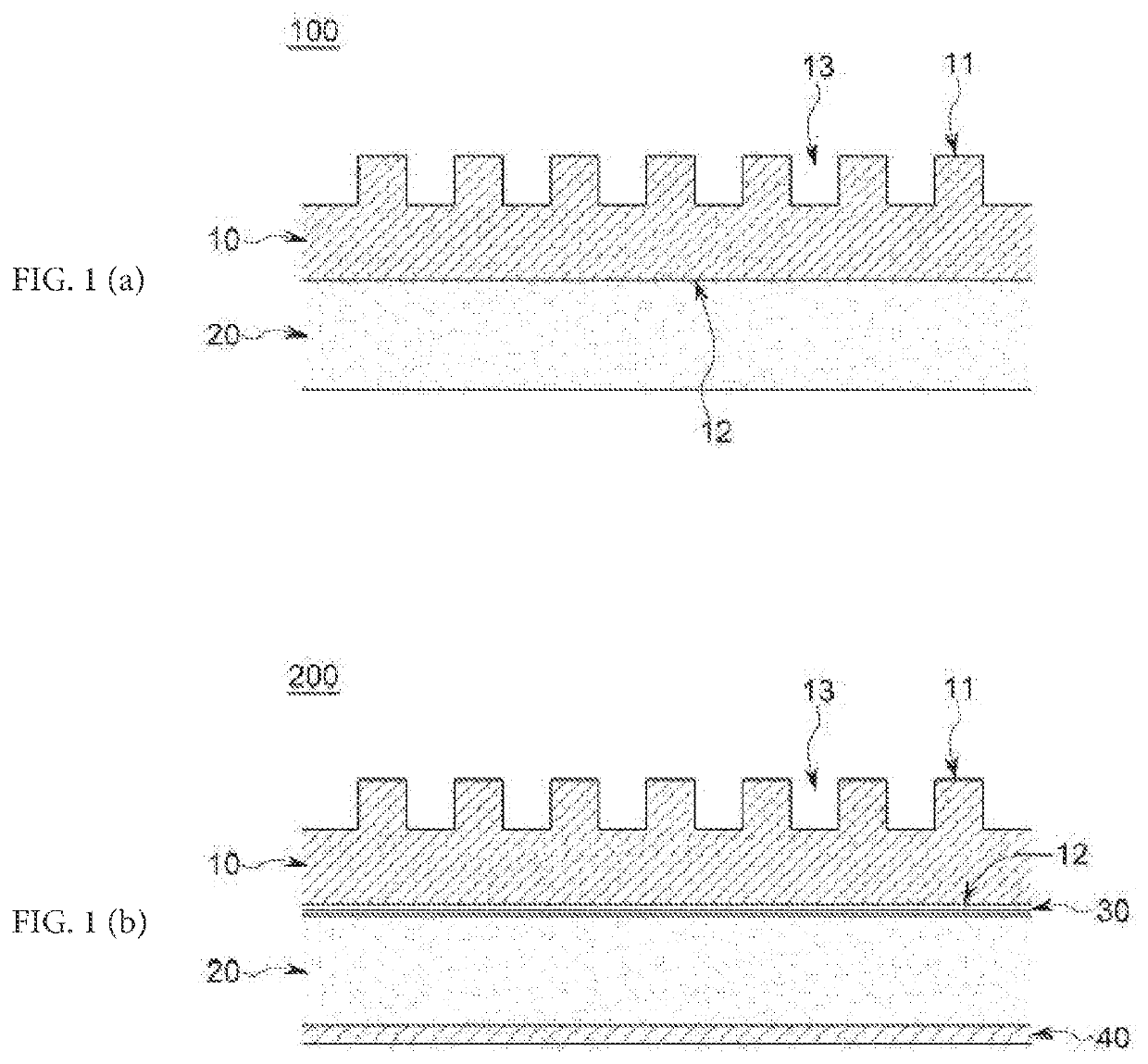
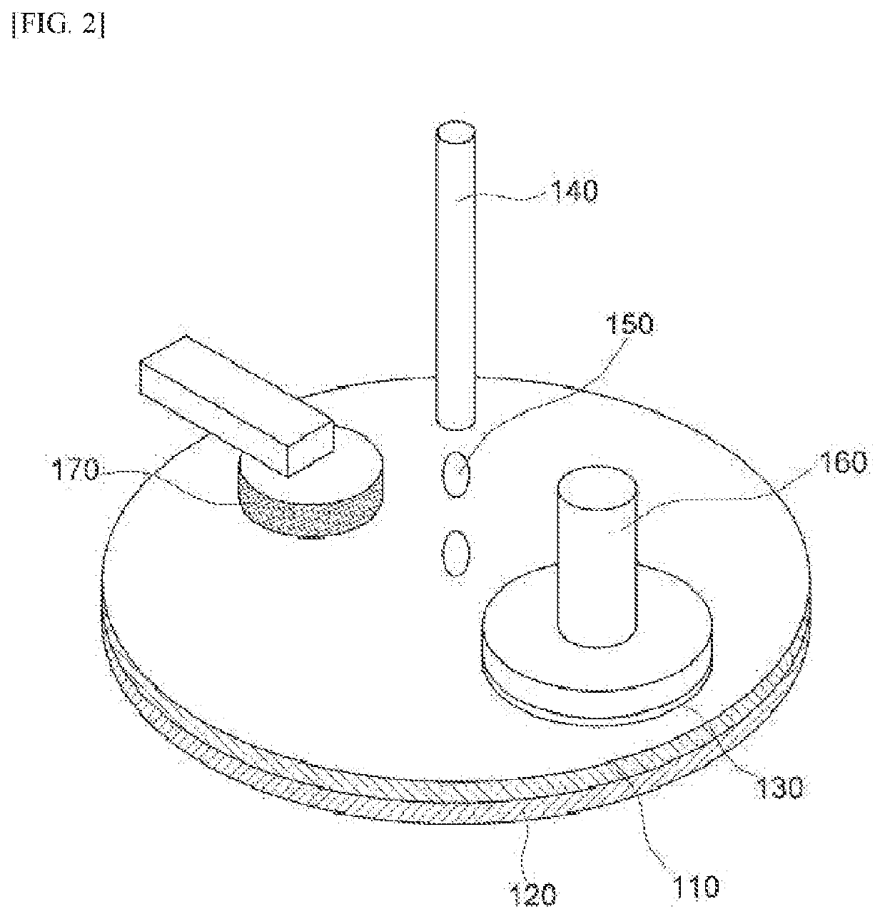
CROSS-REFERENCE TO RELATED APPLICATION(S)[0001]This application claims priority to Korean Patent Application No. 10-2020-0126784, filed on Sep. 29, 2020 and No. 10-2020-0128580, filed on Oct. 6, 2020, the disclosure of which is incorporated herein by reference in its entirety.TECHNICAL FIELD[0002]The present disclosure relates to a pad which is applied to a polishing process, and to a technique for applying this pad to a method for fabricating a semiconductor device.DESCRIPTION OF THE RELATED ART[0003]A chemical mechanical planarization (CMP) or chemical mechanical polishing (CMP) process may be performed for various purposes in various technical fields. The CMP process is performed on a predetermined polishing target surface of a polishing target, and may be performed for the purposes of planarization of the polishing target surface, removal of aggregated materials, reduction of crystal lattice damage, and removal of scratches and contamination sources.[0004]CMP process technologie...

Claims


Application Information

Patent Timeline
Patent Type & Authority Applications(United States)
IPC IPC(8): B24B7/22H01L21/3105
CPCB24B7/228H01L21/31053B24B37/24
Inventor JOENG, EUN SUNYUN, JONG WOOKKYUN, MYUNG OKSEO, JANG WONRYU, JI YEON
Owner SK ENPULSE CO LTD
Learn More